A chip bonding method and ultrasonic indenter design for rapid generation of high melting point joints
A chip bonding and high melting point technology, applied in the field of materials, can solve problems such as device damage and chip cracking, and achieve the effects of enhancing wettability, improving production efficiency, and reducing production costs
- Summary
- Abstract
- Description
- Claims
- Application Information
AI Technical Summary
Problems solved by technology
Method used
Image


Examples
Embodiment 1
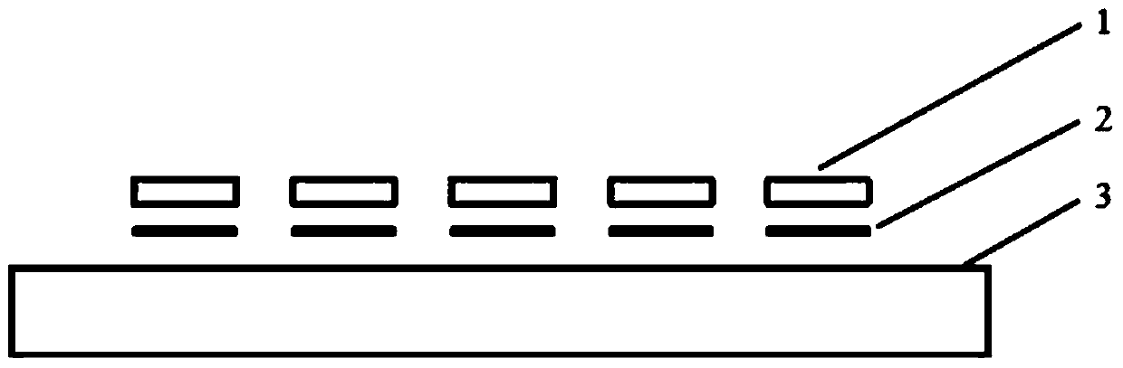
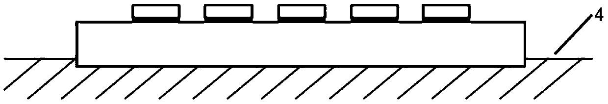
[0052] See attached figure 1 , 2 , Shown in 3, a kind of chip bonding method of fast generation high melting point joint, connecting material comprises base material one (1), intermediate layer two (2) and base material three (3), and this bonding method comprises the following steps:
[0053] I. Surface treatment of the materials to be connected: mechanically polish the base material one (1), the middle layer (2) and the base material three (3) to ensure the removal of surface oil and attachments, and ultrasonically clean the raw materials after grinding 1 to 5 minutes;
[0054] II. Place base material three (3) on the lower layer, base material one (1) on the upper layer and the middle layer (2) in the middle to form a "sandwich" structure;
[0055] III. Heat the base material three (3) with a heating device, and make the middle layer two (2) reach a predetermined melting temperature of 240-260°C through heat conduction;
[0056] IV. The ultrasonic vibration indenter 5 ac...
Embodiment 2
[0069] See attached figure 1 , 2 , 3, a chip bonding method and ultrasonic indenter design for quickly generating high melting point joints, the connecting materials include base material one (1), intermediate layer two (2) and base material three (3), the bond The combination method includes the following steps:
[0070] I. Surface treatment of the materials to be connected: mechanically polish the base material one (1), the middle layer (2) and the base material three (3) to ensure the removal of surface oil and attachments, and ultrasonically clean the raw materials after grinding 1 to 5 minutes;
[0071] II. Place base material three (3) on the lower layer, base material one (1) on the upper layer and the middle layer (2) in the middle to form a "sandwich" structure;
[0072] III. Heat the base material three (3) with a heating device, and make the middle layer two (2) reach a predetermined melting temperature of 240-260°C through heat conduction;
[0073] IV. The ultr...
Embodiment 3
[0087] See attached figure 1 , 2 , 3, a chip bonding method and ultrasonic indenter design for quickly producing high-melting point joints, the connecting materials include base material one (1), intermediate layer two (2) and base material three (3), the bonding The method includes the following steps:
[0088] I. Surface treatment of the materials to be connected: mechanically polish the base material one (1), the middle layer (2) and the base material three (3) to ensure the removal of surface oil and attachments, and ultrasonically clean the raw materials after grinding 1 to 5 minutes;
[0089] II. Place base material three (3) on the lower layer, base material one (1) on the upper layer and the middle layer (2) in the middle to form a "sandwich" structure;
[0090] III. Heat the base material three (3) with a heating device, and make the middle layer two (2) reach a predetermined melting temperature of 240-260°C through heat conduction;
[0091] IV. The ultrasonic vib...
PUM
| Property | Measurement | Unit |
|---|---|---|
| thickness | aaaaa | aaaaa |
| melting point | aaaaa | aaaaa |
| diameter | aaaaa | aaaaa |
Abstract
Description
Claims
Application Information
 - Generate Ideas
- Intellectual Property
- Life Sciences
- Materials
- Tech Scout
- Unparalleled Data Quality
- Higher Quality Content
- 60% Fewer Hallucinations
Browse by: Latest US Patents, China's latest patents, Technical Efficacy Thesaurus, Application Domain, Technology Topic, Popular Technical Reports.
© 2025 PatSnap. All rights reserved.Legal|Privacy policy|Modern Slavery Act Transparency Statement|Sitemap|About US| Contact US: help@patsnap.com