Substrate repairing device and repairing method

A substrate repair and substrate technology, applied in nonlinear optics, instruments, optics, etc., can solve the problems of abrasive belt breakage, long repair time, and low efficiency, and achieve the effects of avoiding waste, reducing loss rate, and improving repair efficiency

Active Publication Date: 2015-09-02
HEFEI BOE OPTOELECTRONICS TECH +1
View PDF3 Cites 10 Cited by
  • Summary
  • Abstract
  • Description
  • Claims
  • Application Information

AI Technical Summary

Problems solved by technology

[0004] In the above-mentioned repairing method, a grinding belt with aluminum powder attached to the PET (polyethylene) film is used to grind it repeatedly, and the black defect after being ground will have over-grinding (grinding the black defect into a white defect similar to a pin hole) ) and the grinding ring / grinding color is light (grinding black defects into similar light and white defects); when the black defects are hard foreign objects such as metals, the grinding belt is likely to break during the grinding process. At the same time, the used It is difficult to recycle the grinding belt, and it needs to be adjusted again after replacing the grinding belt, resulting in long repair time and low efficiency; this will affect the repair quality of black defects and the smooth progress of the grinding repair process

Method used


Image

  • Substrate repairing device and repairing method
  • Substrate repairing device and repairing method
  • Substrate repairing device and repairing method

Examples


Embodiment Construction

[0030] The specific implementation manners of the present invention will be further described below in conjunction with the drawings and examples. The following examples are only used to illustrate the technical solution of the present invention more clearly, but not to limit the protection scope of the present invention.

[0031] In one embodiment of the present invention, a substrate repairing device is provided.

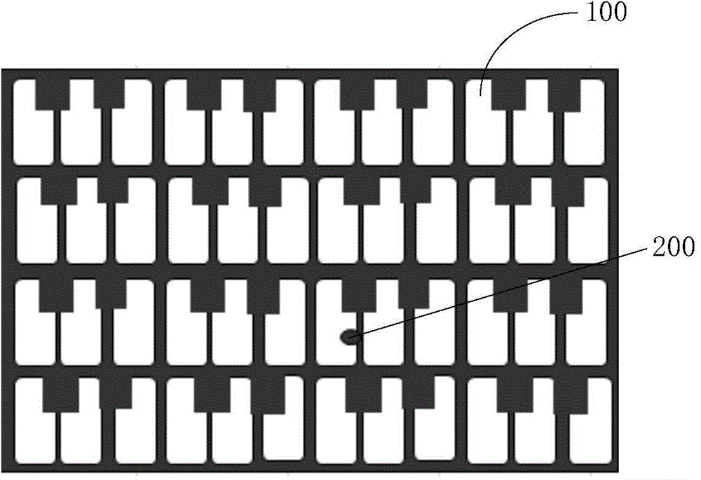
[0032] Figure 4 A schematic diagram of the substrate repairing device of the present invention is shown. Figure 5 A schematic diagram showing the repairing of the substrate by the first laser of the substrate repairing device of the present invention.

[0033] refer to Figure 4 and Figure 5 , the substrate repairing device provided by the present invention specifically includes a laser emitter 201 and an imaging unit 202 .

[0034] In this embodiment, the laser emitter 201 is located on one side of the substrate, and the laser emitter 201 can emit a first...


PUM

PropertyMeasurementUnit
wavelengthaaaaaaaaaa

Abstract

The invention provides a substrate repairing device and a repairing method. The device comprises a laser emitter and an imaging unit. Being located on one side of a substrate, and with a preset height from the surface of the substrate, the laser emitter emits a first laser which is in parallel with the surface of the substrate and is used for detecting protruded defects of the substrate, and emits a second laser which is used for repairing the protruded defects requiring repair. The imaging unit is used for imaging the substrate; when it is detected that the first laser is scattered by certain protruded defects, the protruded defects are judged to be the protruded defects requiring the repair. By using the low-energy laser to detect the protruded defects and using the high-energy laser to repair the protruded defects, the substrate repairing device can efficiently repair the protruded defects of the substrate.

Description

technical field [0001] The invention relates to the field of display technology, in particular to a substrate repairing device and a repairing method. Background technique [0002] At present, in the production process of color filters in the TFT-LCD industry, black defects (foreign objects, etc.) and white defects (missing pixels, etc.) often occur during the production process. The existing defect repair method is to use a graphic correction machine to repair, such as laser Irradiation, Tape grinding, and Ink coating (using pigments similar to color photoresist to fill missing pixel parts) repair, etc. [0003] For color filter surface protrusions (highly black defects), such as figure 1 As shown, when repairing, the position of each protruding defect 200 on the substrate 100 is first searched, and then each protruding defect is measured by a measuring sensor to obtain the height 201 of each protruding defect, as shown in figure 2 A three-dimensional schematic of a prot...

Claims


Application Information

Patent Timeline
Patent Type & Authority Applications(China)
IPC IPC(8): G02F1/13
CPCG02F1/1309
Inventor 胡瑾节昌凯孟祥明李坤
Owner HEFEI BOE OPTOELECTRONICS TECH
Why Eureka
Try Eureka