TSV (through silicon via) electrical characteristic measuring structure based on de-embedding method

A through-silicon via and de-embedding technology, which is applied to the measurement structure of the integrated circuit through-silicon via, and in the field of measuring the electrical characteristics of the through-silicon via based on the de-embedding method, can solve the problem of increasing errors, increasing method errors, and failure to maintain electrical characteristics Invariant and other problems, to achieve the effect of error reduction

Active Publication Date: 2015-07-22
ZHEJIANG UNIV
View PDF6 Cites 1 Cited by
  • Summary
  • Abstract
  • Description
  • Claims
  • Application Information

AI Technical Summary

Problems solved by technology

However, this method is based on the ideal condition of formula (2), that is, the vertical interconnection and the horizontal interconnection do not affect each other, and the electrical characteristics of the two remain unchanged after the connection, but in the microwave and millimeter wave frequency bands, the strong electromagnetic coupling between the two Make them unable to keep their respective electrical characteristics unchanged, this condition cannot be satisfied, and then greatly increases the error of the whole method, such as figure 1 shown
[0016] Therefore, in the microwave and millimeter wave frequency bands, there is a strong electromagnetic coupling between the vertical TSVs and the horizontal interconnection structure, and they affect each other, which greatly increases the error of the above method

Method used


Image

  • TSV (through silicon via) electrical characteristic measuring structure based on de-embedding method
  • TSV (through silicon via) electrical characteristic measuring structure based on de-embedding method
  • TSV (through silicon via) electrical characteristic measuring structure based on de-embedding method

Examples


Embodiment Construction

[0043] The present invention will be further described below in conjunction with drawings and embodiments.

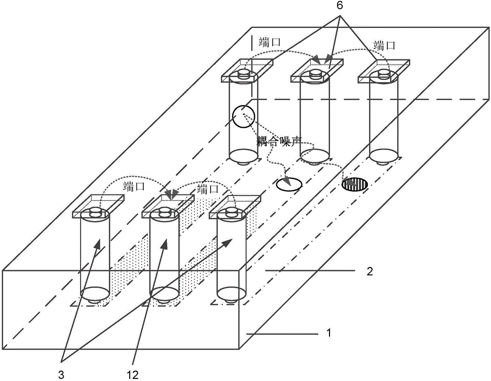
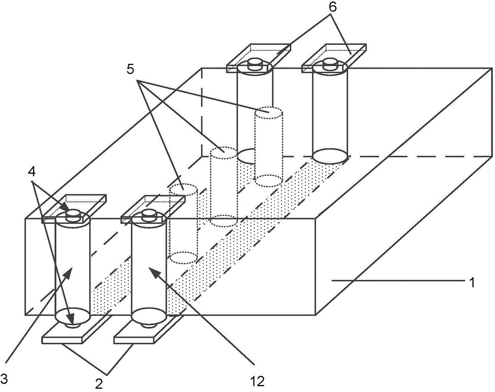
[0044] Such as figure 2As shown, the measurement structure of the present invention includes a silicon substrate 1, a bottom RDL (Redistribution Layer, rewiring layer) conductor 2, a TSV (Through Silicon Via, TSV) structure to be tested connected by the bottom RDL conductor 2, bumps 4 and test Pin 6, the TSV structure to be tested is composed of two sets of TSV columns to be tested symmetrically distributed on both sides. The TSV structure to be tested includes the signal TSV structure 3 to be tested and the ground TSV structure 12 to be tested. , and it is isolated from the silicon substrate 1 by insulating materials such as the structural oxide insulating layer 7 , the top substrate insulating layer 8 , and the bottom substrate insulating layer 9 .

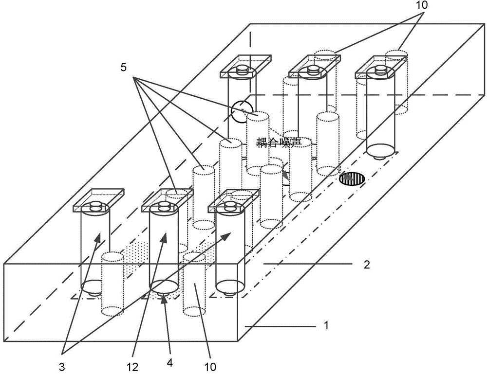
[0045] Such as image 3 , 4 As shown, for two-port and multi-port interconnection structures, an isolation TSV stru...


PUM


Abstract

The invention discloses a TSV (through silica via) electrical characteristic measuring structure based on a de-embedding method. As for a two-port and multi-port interconnecting structure, TSV isolation structures are arranged on perpendicular divide lines of central connection lines of to-be-measured signal TSV structures and to-be-measured ground TSV structures on the same sides, used for isolating electromagnetic coupling of perpendicular to-be-measured TSV structures with horizontal bottom RDL (redistribution layer) conductors, mainly comprise metal through silicon via columns arranged at intervals, and include inner TSV isolation structures or include the inner TSV isolation structures and outer TSV isolation structures. The TSV electrical characteristic measuring structure is completely compatible with an existing through silicon via production technology, suitable for measuring electrical characteristics of micrometer-waveband and millimeter-waveband through silicon vias by the de-embedding experimental measurement method and higher in measuring precision as compared with a traditional measuring method, and has great application value in the field of micrometer-waveband and millimeter-waveband three-dimensional structure measurement.

Description

technical field [0001] The present invention relates to a measurement structure of integrated circuit through-silicon vias, in particular to a measurement structure for measuring the electrical characteristics of through-silicon vias based on the de-embedding method in the field of microwave and millimeter-wave device testing, which weakens the through-silicon vias and their connections The coupling noise of the horizontal interconnection lines can significantly improve the accuracy of the electrical characteristics measured by the de-embedding method. Background technique [0002] At present, the design of mainstream integrated circuits, including Intel's multi-chip architecture, continues the traditional two-dimensional flat system architecture. Limit constraints call for the emergence of a new integrated circuit system architecture in order to fully reflect its three-dimensional vertical scale—this is the three-dimensional integrated circuit. Three-dimensional integrated...

Claims


Application Information

Patent Timeline
Patent Type & Authority Applications(China)
IPC IPC(8): G01R31/26
Inventor 李尔平李永胜杨德操魏兴昌
Owner ZHEJIANG UNIV
Why Eureka
Try Eureka