A three-dimensional coupler based on through-silicon via and its preparation method

A technology of couplers and through-silicon vias, which is applied in the field of three-dimensional couplers based on through-silicon vias and their preparation, can solve the problem that discrete three-dimensional microwave couplers are difficult to meet the integration requirements, the directional adjustable space is small, and it occupies a large chip area. problems, to achieve the effect of simplifying the electromagnetic isolation design, small influence of electromagnetic characteristics, and small footprint

Active Publication Date: 2021-05-28
XIDIAN UNIV
View PDF7 Cites 0 Cited by
  • Summary
  • Abstract
  • Description
  • Claims
  • Application Information

AI Technical Summary

Problems solved by technology

The traditional planar microwave coupler not only occupies a huge chip area, but also has little room for adjustment of coupling degree, directivity and other indicators, especially the isolation degree is difficult to improve
In addition, discrete three-dimensional microwave couplers based on low-temperature co-fired ceramic technology are difficult to meet the requirements of integration

Method used


Image

  • A three-dimensional coupler based on through-silicon via and its preparation method
  • A three-dimensional coupler based on through-silicon via and its preparation method
  • A three-dimensional coupler based on through-silicon via and its preparation method

Examples


Embodiment Construction

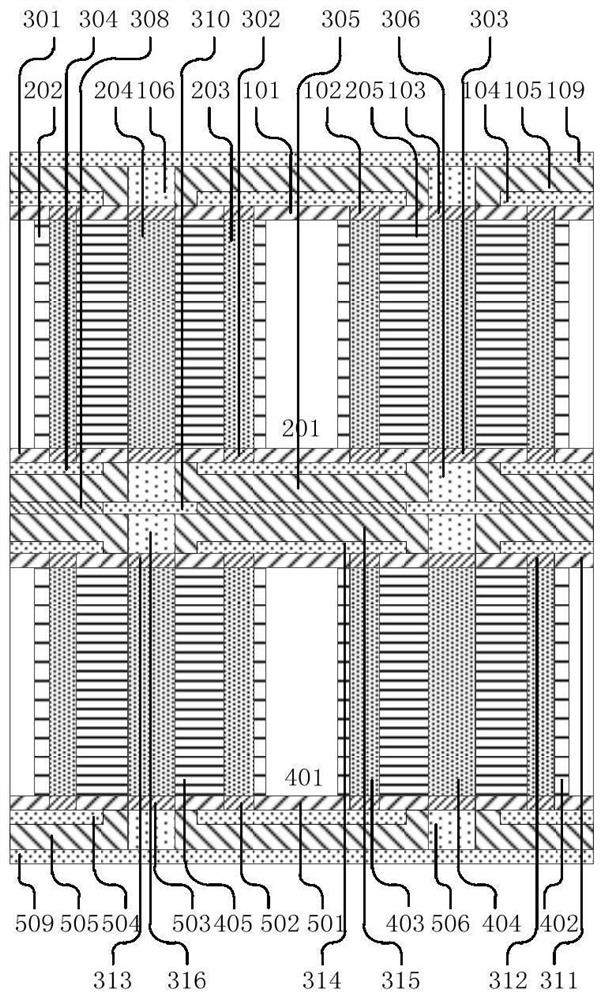
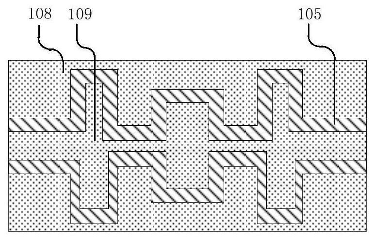
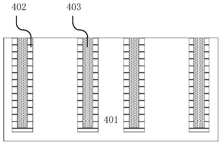
[0122] As shown in Figure 1, a three-dimensional coupler based on through-silicon vias provided by an embodiment of the present invention includes a top ground layer 108, a top signal line 109, a top dielectric layer 105, a top ground column 107, a top signal line Interconnection columns 106, top and bottom ground layers 104, top and bottom dielectric layers 101, top and bottom signal interconnection columns 103, top and bottom shielding layers 102, upper silicon substrate 201, upper first dielectric layer 202, upper shielding layer 203, upper The second dielectric layer 205, the upper signal interconnection column 204, the first dielectric layer 301 at the top of the middle layer, the shielding layer 302 at the top of the middle layer, the first signal interconnection column 303 at the top of the middle layer, the ground layer 304 at the top of the middle layer, and the top of the middle layer The second dielectric layer 305, the second signal interconnection column 306 at the...


PUM


Abstract

The invention discloses a three-dimensional coupler based on through-silicon vias and a preparation method thereof, which relate to the field of three-dimensional integrated circuits, mainly through the use of three-dimensional integration technology of through-silicon vias and a multi-node structure, combined with reactive ion etching technology and electrochemical deposition , Plasma-enhanced chemical vapor deposition and chemical vapor deposition methods, etc., effectively reduce the length of interconnection lines and chip area, improve data transmission bandwidth and integration, and realize the simultaneous improvement of integrated circuit performance and reduce The purpose of power consumption, weight reduction and volume reduction solves the shortcomings of existing technologies, such as large occupied chip area, small adjustable space for coupling, orientation and other indicators, especially the difficulty of improving isolation and meeting the requirements of integration.

Description

technical field [0001] The invention belongs to the field of three-dimensional integrated circuits, and in particular relates to a three-dimensional coupler based on through-silicon holes and a preparation method thereof. Background technique [0002] Three-dimensional integration technology distributes the functional modules of the circuit system on different chips (which can be chips with different functions and different processes), and forms a three-dimensional stack through low-temperature bonding. In a three-dimensional integrated circuit (3-Dimension Integrated Circuit, 3-D IC), the electrical connection between the upper and lower modules is realized through a through-silicon via (TSV), which has a decisive effect on the performance of the entire system. 3-D IC has the advantages of being able to greatly reduce the global interconnect length, increase data transmission bandwidth, reduce chip area, increase integration, and realize chip heterogeneous integration. It c...

Claims


Application Information

Patent Timeline
Patent Type & Authority Patents(China)
IPC IPC(8): H01P5/16H01P11/00H01L23/528H01L21/768
CPCH01L21/76801H01L21/76838H01L23/528H01L23/5286H01P5/16H01P11/00
Inventor 卢启军朱樟明杨银堂李跃进丁瑞雪
Owner XIDIAN UNIV
Why Eureka
Try Eureka