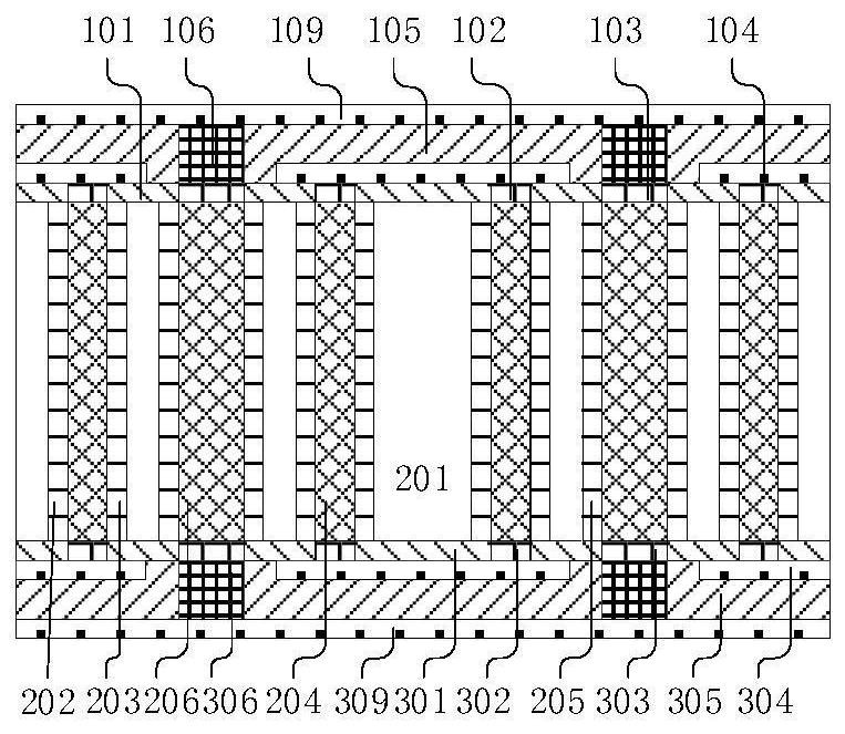
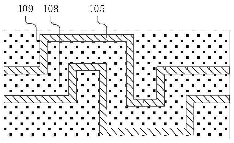
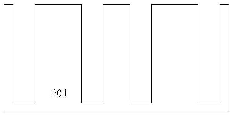
Three-dimensional hybrid ring coupler based on through silicon via
A three-dimensional hybrid and coupler technology, which is applied to waveguide devices, electric solid devices, semiconductor devices, etc., can solve problems such as difficulty in applying microwave and millimeter wave frequency bands, difficulty in meeting integration requirements, and large chip area. Electromagnetic isolation characteristics, reducing the influence of electromagnetic characteristics, and good compatibility
- Summary
- Abstract
- Description
- Claims
- Application Information
AI Technical Summary
Problems solved by technology
Method used
Image

Examples
Embodiment Construction
[0037] In order to make those skilled in the art better understand the technical solutions of the present invention, the technical solutions in the embodiments of the present invention will be clearly and completely described below with reference to the embodiments of the present invention and the accompanying drawings. Obviously, the described embodiments are only some, but not all, embodiments of the present invention. Based on the embodiments of the present invention, all other embodiments obtained by persons of ordinary skill in the art without creative efforts shall fall within the protection scope of the present invention.
[0038] It should be understood that the specific embodiments described herein are only used to further explain the present invention, and are not intended to limit the present invention. In the following description, the use of sequential words used to indicate the distinction of elements, such as "first", "second", "third", etc., is only for the des...
PUM
 Abstract
Description
Claims
Application Information
 - R&D Engineer
- R&D Manager
- IP Professional
- Industry Leading Data Capabilities
- Powerful AI technology
- Patent DNA Extraction
Browse by: Latest US Patents, China's latest patents, Technical Efficacy Thesaurus, Application Domain, Technology Topic.
© 2024 PatSnap. All rights reserved.Legal|Privacy policy|Modern Slavery Act Transparency Statement|Sitemap