A detection structure and detection method for wafer bonding quality

A detection structure, wafer bonding technology, applied in the direction of semiconductor/solid-state device testing/measurement, electrical components, electric solid-state devices, etc., can solve problems such as inability to accurately measure bonding contact resistance, inability to accurately reflect bonding, etc. , to achieve the effect of simple test structure

Active Publication Date: 2018-08-21
SEMICON MFG INT (SHANGHAI) CORP
View PDF6 Cites 1 Cited by
  • Summary
  • Abstract
  • Description
  • Claims
  • Application Information

AI Technical Summary

Problems solved by technology

[0005] At present, the quality inspection of Cu-Cu bonding (wafer level Cu-Cu bonding) at the wafer level mainly uses the traditional resistance chain (Rc chain) method to test, such as figure 1 As shown, but the Rc in the traditional resistance chain (Rc chain) test includes the resistance of the joint (bonding), the metal layer metal, and the via (Via), Rc=R bonding +R Via +R metal , and the resistance value brought by normal bonding (bonding) accounts for a small proportion in Rc, only when the bonding quality (bonding quality) is poor, it can qualitatively reflect the quality of bonding (bonding), but it cannot be accurate The measurement of the contact resistance of the bonding itself cannot accurately reflect the quality of the bonding
[0006] Although there is a detection structure for the quality detection of Cu-Cu bonding at the wafer level (wafer level Cu-Cubonding) in the prior art, there are still various deficiencies. How to effectively detect the quality and yield of bonding (bonding) online , how to accurately measure the junction resistance R bonding become an urgent problem to be solved

Method used


Image

  • A detection structure and detection method for wafer bonding quality
  • A detection structure and detection method for wafer bonding quality
  • A detection structure and detection method for wafer bonding quality

Examples


Embodiment 1

[0054] The test structure of the present invention will be further described below in conjunction with the accompanying drawings.

[0055] First, refer to Figure 2a-2b , in the test structure, including a semiconductor substrate 201, the semiconductor substrate 201 may be at least one of the materials mentioned below: silicon, silicon-on-insulator (SOI), silicon-on-insulator (SSOI) , Silicon germanium on insulator (S-SiGeOI), silicon germanium on insulator (SiGeOI) and germanium on insulator (GeOI), etc. Active regions may be defined on the semiconductor substrate.

[0056] The test structure includes a bottom wafer 30 and a top wafer 40 bonded to each other, the bottom wafer 30 and the top wafer 40 are bonded to each other through pads, and the bonding of the pads includes a plurality of mutually isolated solder pads. pad, wherein, in the bottom wafer 30, it includes a first bottom pad 202, a second bottom pad 203, and a third bottom pad 204, and a first bottom pad 204 is ...

Embodiment 2

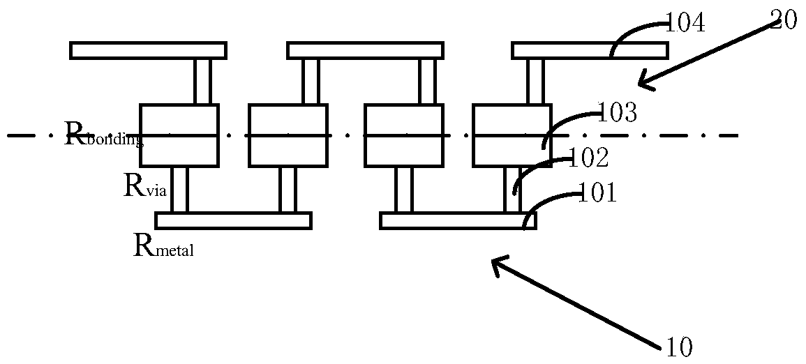
[0080] The present invention also provides a method for selecting the above test structure to detect the bonding of the bottom wafer and the top wafer, wherein image 3 It is an equivalent circuit diagram of the detection structure of the wafer bonding quality in a specific implementation manner.

[0081] The methods include:

[0082] Step (a) applying a voltage on the first test terminal and the third test terminal, testing the voltage between the third test terminal and the fourth test terminal, and calculating a resistance value R1;

[0083] Step (b) applying a voltage on the third test terminal and the fifth test terminal, testing the voltage between the fourth test terminal and the sixth test terminal, and calculating the resistance value R2;

[0084] Step (c) calculating a junction resistance between said third top pad and said third bottom pad based on R1 and R2.

[0085] Specifically, the step (c) also includes the following sub-steps:

[0086] Step (c-1) said R1=R ...


PUM


Abstract

The invention relates to a detection structure and a detection method for detecting the quality of wafer bonding. According to the detection structure, a bottom metal layer, bottom pads, and bottom through holes between the bottom metal layer and the bottom pads of a bottom wafer form an interconnect structure which is used as a lower half part of the test structure; top pads, a top metal layer, and top through holes between the top pads and the top metal layer of a top wafer form an interconnect structure which is used as an upper half part of the test structure; and the top metal layer is used as a test pad, and the opening of the test pad is arranged in the top metal layer of the top wafer after the top wafer is thinned. The test structure is composed of three parts, wherein the left and right test structures are respectively a first test target and a second test target, and the middle structure mainly plays a lead role. The test structure is a symmetrical structure, which enables other additional resistors except the test targets in the circuit to be equal. By adopting the test structure of the invention, the problem that the Cu-Cu bonding resistance Rc in a 3D IC cannot be tested accurately is solved simply and effectively.

Description

technical field [0001] The invention relates to the field of semiconductors, in particular, the invention relates to a wafer bonding quality detection structure and detection method. Background technique [0002] In the field of electronic consumption, multi-function devices are more and more popular among consumers. Compared with devices with simple functions, the production process of multi-function devices will be more complicated, such as the need to integrate multiple chips with different functions on the circuit board, so 3D integrated circuit (integrated circuit, IC) technology, 3D integrated circuit (integrated circuit, IC) is defined as a system-level integrated structure, stacking multiple chips in the vertical plane direction, thereby saving space, the edge of each chip Multiple pins can be drawn out as needed, and these pins can be used to interconnect the chips that need to be connected to each other through metal wires, but the above method still has many short...

Claims


Application Information

Patent Timeline
Patent Type & Authority Patents(China)
IPC IPC(8): H01L23/544H01L21/66
Inventor 戚德奎陈政李新
Owner SEMICON MFG INT (SHANGHAI) CORP
Why Eureka
Try Eureka