Structures and manufacturing methods of or logic and nand logic devices

A logic device, non-logic technology, applied in the field of integrated circuit manufacturing, can solve the problems of high cost, complex circuit structure, large chip area, etc., achieve simple timing control, simple device and circuit structure, and reduce circuit signal delay. Effect

Inactive Publication Date: 2015-07-01
SHANGHAI HUAHONG GRACE SEMICON MFG CORP
View PDF6 Cites 0 Cited by
  • Summary
  • Abstract
  • Description
  • Claims
  • Application Information

AI Technical Summary

Problems solved by technology

[0004] The disadvantages of these two logic circuits are that the circuit structure is complex, the chip area is large, and the cost is high.

Method used


Image

  • Structures and manufacturing methods of or logic and nand logic devices
  • Structures and manufacturing methods of or logic and nand logic devices
  • Structures and manufacturing methods of or logic and nand logic devices

Examples


Embodiment Construction

[0038] In order to have a more specific understanding of the technical content, characteristics and effects of the present invention, now in conjunction with the accompanying drawings, the details are as follows:

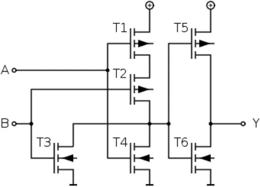
[0039] OR logic device structure of the present invention, see image 3 , 4 shown.

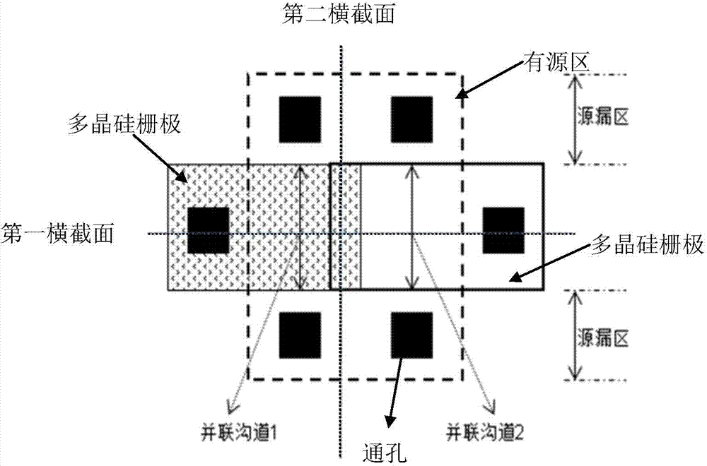
[0040] Or logic devices, fabricated in a p-well or p-type substrate, with two parallel and adjacent gate gates on it, each controlling the adjacent n-type conduction channel below it. In the direction along the boundary line between the two gate control gates, there is an n-type source region and a drain region at both ends of the gate control gate. In this way, two parallel n-type channels are formed by using the source and drain as leads. There is a polysilicon gate on each of the two gates. The two polysilicon gates can be spaced apart, adjacent to each other or overlap each other, but they must be electrically isolated from each other and independently drawn out as two input ...


PUM


Abstract

The invention discloses structures of or logic and nand logic devices. The or logic device is manufactured in a grounded p well or p type substrate, and two parallel and close door control gates are arranged on the upper side to control two adjacent and parallel n-type conductive trenches on the lower side respectively; a highly doped n type source region and drain region are arranged at the two ends of the door control gates along the direction of the boundary of the two door control gates to serve as lead-out ends of the two trenches; a polycrystalline gate is arranged on each door control gate; the two polycrystalline silicon gates are mutually electrically isolated and led out independently to serve as two input ends of or logic; the structures of the nand logic device and the or logic device are similar; the difference is that the nand logic device and the or logic device are manufactured in the n well or the n type substrate, and the source and drain regions are highly doped p type. The invention also discloses manufacturing methods of the or and nand logic devices of the structures. By designing the novel or and nand logic device structures, the devices and the circuit structures are simplified, the circuit area and the manufacturing cost are reduced, and the time sequence control of the circuit is simpler.

Description

technical field [0001] The invention relates to the field of integrated circuit manufacturing, in particular to the structure of OR logic and NAND logic devices and its manufacturing method. Background technique [0002] Traditional OR gate logic circuits are implemented using 6 MOS (metal oxide semiconductor) transistors, including 3 nMOS (n-well channel metal oxide semiconductor) and 3 pMOS (p-type channel metal oxide semiconductor), such as figure 1 shown. The working principle of the traditional OR gate logic circuit is: when the two input terminals A and B are both low potential "0", the output terminal Y is low potential "0"; otherwise, the output terminal Y is high potential "1". [0003] The traditional NAND gate logic circuit is implemented using 4 MOS transistors, including one nMOS and two pMOS, such as figure 2 shown. The working principle of the traditional NAND gate logic circuit is: when the two input terminals A and B are both high potential "1", the outp...

Claims


Application Information

Patent Timeline
Patent Type & Authority Applications(China)
IPC IPC(8): H01L27/02H01L27/088H01L29/423H01L21/8234H01L21/28H03K19/173
Inventor 吴兵王永成戴有江
Owner SHANGHAI HUAHONG GRACE SEMICON MFG CORP
Why Eureka
Try Eureka