Oxide sintered body, oxide sputtering target and conductive oxide thin film with high refractive index, and method for producing oxide sintered body
A manufacturing method and technology of sintered body, which can be applied to conductive layers on insulating carriers, sputtering plating, ion implantation plating, etc., can solve problems such as difficulty in using plastic substrates, organic EL devices, etc., to improve productivity and reduce equipment. Cost, effect of high refractive index
- Summary
- Abstract
- Description
- Claims
- Application Information
AI Technical Summary
Problems solved by technology
Method used
Image
Examples
Embodiment 1
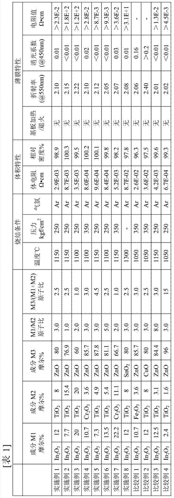
[0060] Ready In 2 o 3 Powder, TiO 2 powder, ZnO powder, and these powders were formulated and mixed in the compounding ratio described in Table 1. Next, the mixed powder was heated under an argon atmosphere at a temperature of 1150°C and a pressure of 250kgf / cm 2 hot-pressed sintering conditions. Then, the sintered body is machined and finished into a target shape.
[0061] Next, sputtering was performed using the 6-inch-diameter target obtained by the above finishing process. The sputtering conditions were set as DC sputtering, sputtering power 500W, argon gas pressure 0.5Pa containing 0-2 vol% oxygen, and the film was formed to a film thickness of In addition, substrate heating during sputtering and annealing after sputtering are performed.
[0062] The results are shown in Table 1. As shown in Table 1, the relative density of the sputtering target reaches 98.9%, and the bulk resistance is 2.9×10 -3 Ω·cm, capable of stable DC sputtering. Moreover, the refractive in...
Embodiment 2
[0065] Ready In 2 o 3 Powder, TiO 2 powder, ZnO powder, and these powders were formulated and mixed in the compounding ratio described in Table 1. Next, the mixed powder was heated under an argon atmosphere at a temperature of 1150°C and a pressure of 250kgf / cm 2 hot-pressed sintering conditions. Then, the sintered body is machined and finished into a target shape. Next, sputtering was performed under the same conditions as in Example 1 using the 6-inch-diameter target obtained by the above finishing process. As a result, the relative density of the sputtering target reached 100.3%, and the bulk resistance was 8.7×10 -3 Ω·cm, capable of stable DC sputtering. Moreover, the film obtained by sputtering has a refractive index of 2.15 (wavelength 550nm), an extinction coefficient of less than 0.01 (wavelength 450nm), and a resistance value of 1.8×10 +2 Ω·cm or more, a conductive film with high refractive index and high transmittance was obtained.
Embodiment 3
[0067] Ready In 2 o 3 Powder, TiO 2 powder, ZnO powder, and these powders were formulated and mixed in the compounding ratio described in Table 1. Next, the mixed powder was heated under an argon atmosphere at a temperature of 1100°C and a pressure of 250kgf / cm 2 hot-pressed sintering conditions. Then, the sintered body is machined and finished into a target shape. Next, sputtering was performed under the same conditions as in Example 1 using the 6-inch-diameter target obtained by the above finishing process. As a result, the relative density of the sputtering target reaches 99.5%, and the bulk resistance is 3.5×10 -3 Ω·cm, capable of stable DC sputtering. Moreover, the film obtained by sputtering has a refractive index of 2.22 (wavelength 550nm), an extinction coefficient of less than 0.01 (wavelength 450nm), and a resistance value of 1.2×10 +2 Ω·cm or more, a conductive film with high refractive index and high transmittance was obtained.
PUM
| Property | Measurement | Unit |
|---|---|---|
| refractive index | aaaaa | aaaaa |
| refractive index | aaaaa | aaaaa |
| refractive index | aaaaa | aaaaa |
Abstract
Description
Claims
Application Information
 - R&D
- Intellectual Property
- Life Sciences
- Materials
- Tech Scout
- Unparalleled Data Quality
- Higher Quality Content
- 60% Fewer Hallucinations
Browse by: Latest US Patents, China's latest patents, Technical Efficacy Thesaurus, Application Domain, Technology Topic, Popular Technical Reports.
© 2025 PatSnap. All rights reserved.Legal|Privacy policy|Modern Slavery Act Transparency Statement|Sitemap|About US| Contact US: help@patsnap.com

