Three-dimensional array-intersected array resistive random access memory and method for manufacturing the memory
A technology of resistive memory and cross array, which is applied to semiconductor devices, electric solid-state devices, electrical components, etc., can solve problems such as blank preparation methods, and achieve the effect of achieving transparency and low manufacturing cost.
- Summary
- Abstract
- Description
- Claims
- Application Information
AI Technical Summary
Problems solved by technology
Method used
Image


Examples
preparation example Construction
[0044] The present invention is an embodiment and also provides a method for preparing a three-dimensional cross-array transparent resistive memory, the method comprising:
[0045] Ultrasonic cleaning of the glass substrate and drying of the cleaned glass substrate;
[0046] Extending and depositing lines of the first transparent oxide lower electrode thin film layer on the glass substrate along the first direction by using a screen printing process;
[0047] Depositing a first transparent oxide resistive layer on the glass substrate and the first transparent oxide lower electrode film layer by using a sol-gel process;
[0048] Using a screen printing process, extending and depositing lines of the first transparent oxide upper electrode thin film layer on the first transparent oxide resistive layer along the second direction;
[0049] Depositing a dielectric isolation layer on the first transparent oxide upper electrode film layer by using a chemical vapor deposition process;...
Embodiment 1
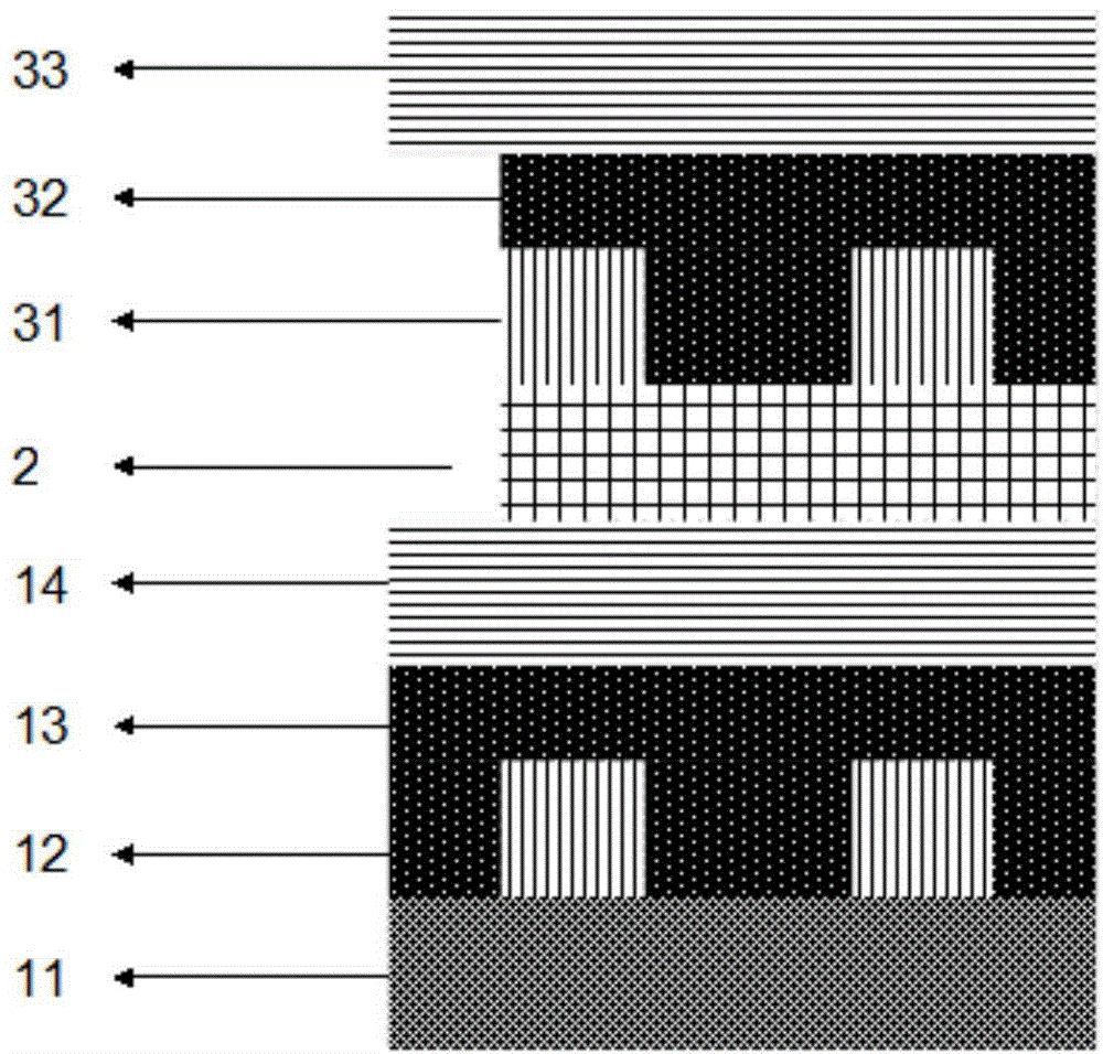
[0055] The transparent oxide electrode layers 12, 14, 31, and 33 in the embodiment of the present invention are Sn-doped indium oxide layer screen-printed films;
[0056] The resistive material in the transparent oxide resistive layer 13, 32 is zirconium dioxide;
[0057] The dielectric isolation layer 21 is organic transparent material parylene (Parylene);
[0058] figure 2 It is a schematic diagram of the processing flow of the preparation method of the three-dimensional cross-array transparent resistive memory in the present invention; wherein, figure 2 The left part of is the front view of the resistive memory during the preparation process of the three-dimensional cross-array transparent resistive memory, figure 2 The right part of is the side view of the resistive memory during the preparation process of the three-dimensional cross-array transparent resistive memory;
[0059] The manufacturing method of the three-dimensional cross-array transparent resistive memory...
Embodiment 2
[0068] The transparent oxide electrode layers 12, 14, 31, 33 in the embodiment of the present invention are Sn-doped indium oxide thin films;
[0069] The resistive material in the transparent oxide resistive layer 13, 32 is zirconium dioxide;
[0070] The dielectric isolation layer 21 is organic transparent material parylene (Parylene);
[0071] The preparation method of the three-dimensional cross-array transparent resistive memory provided in this embodiment is divided into the following steps:
[0072] (1) For example figure 2 The glass substrate in the first step is ultrasonically cleaned in absolute ethanol solution for 10 minutes, and the temperature of the water bath is controlled at about 50°C;
[0073] (2) drying the cleaned glass substrate in an oven, the temperature is controlled at about 60°C;
[0074] (3) Using the sol-gel process, choosing indium nitrate hydrate and stannous chloride hydrate as precursors, absolute ethanol as solvent, and acetylacetone as st...
PUM
| Property | Measurement | Unit |
|---|---|---|
| Thickness | aaaaa | aaaaa |
Abstract
Description
Claims
Application Information
 - R&D Engineer
- R&D Manager
- IP Professional
- Industry Leading Data Capabilities
- Powerful AI technology
- Patent DNA Extraction
Browse by: Latest US Patents, China's latest patents, Technical Efficacy Thesaurus, Application Domain, Technology Topic.
© 2024 PatSnap. All rights reserved.Legal|Privacy policy|Modern Slavery Act Transparency Statement|Sitemap