Array substrate, display panel and display device

A technology of array substrates and substrate substrates, which is applied in the direction of electrical components, electric solid-state devices, circuits, etc., can solve the problems that restrict the development of narrow borders of OLEDs and the width occupied by gate drive circuits, etc.

Active Publication Date: 2017-06-30
BOE TECH GRP CO LTD
View PDF4 Cites 1 Cited by
  • Summary
  • Abstract
  • Description
  • Claims
  • Application Information

AI Technical Summary

Problems solved by technology

However, the gate drive circuit integrated on the array substrate of the OLED still occupies a certain width, which restricts the development of the narrow frame of the OLED.

Method used


Image

  • Array substrate, display panel and display device
  • Array substrate, display panel and display device
  • Array substrate, display panel and display device

Examples


Embodiment Construction

[0042] The specific implementation manners of an array substrate, a display panel and a display device provided by the embodiments of the present invention will be described in detail below with reference to the accompanying drawings.

[0043] The shape and thickness of each film layer in the drawings do not reflect the real proportion of the array substrate, but are only intended to schematically illustrate the content of the present invention.

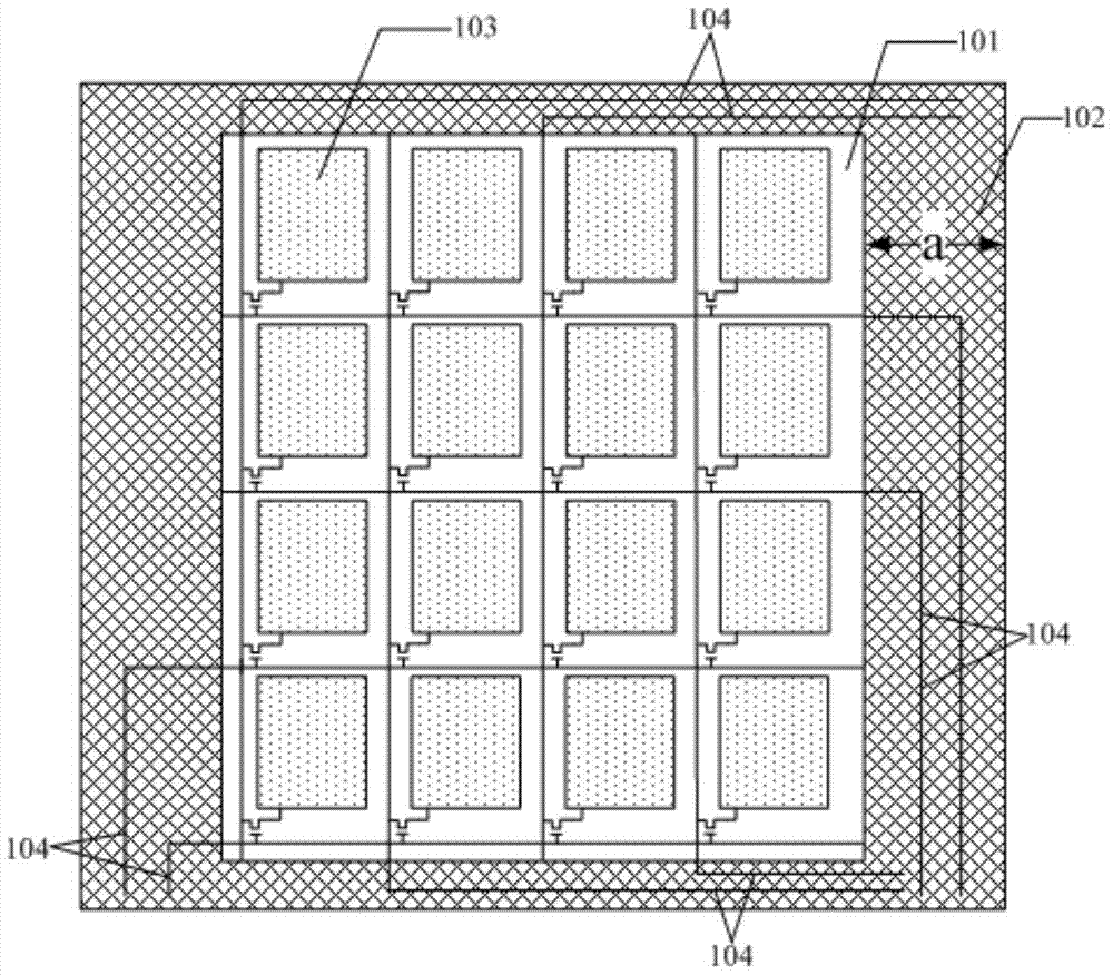
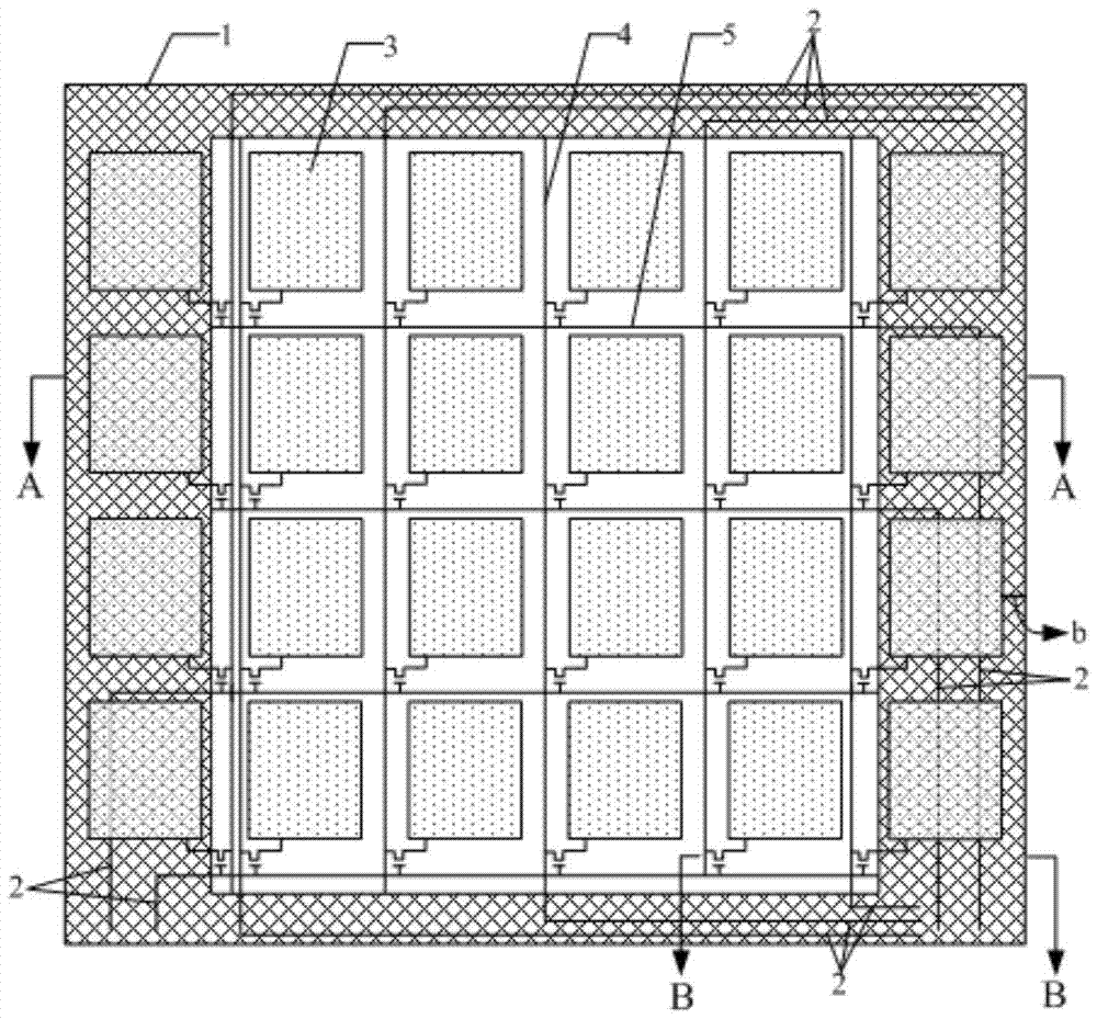
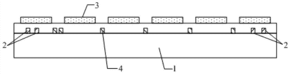
[0044] An array substrate provided by an embodiment of the present invention, such as Figure 2-Figure 5 as shown, image 3 yes figure 2 Sectional view along direction AA, Figure 5 yes Figure 4 A cross-sectional view along the CC direction, including: a base substrate 1, peripheral traces 2 and a plurality of pixel structures 3 located on the base substrate 1;

[0045] The orthographic projection of at least one pixel structure 3 on the base substrate 1 and the peripheral area where the peripheral wiring 2 is located (such as ...


PUM


Abstract

The invention discloses an array substrate, a display panel and a display device. The array substrate includes: a base substrate, peripheral wiring and a plurality of pixel structures located on the base substrate; since at least one pixel structure is located on the base substrate The orthographic projection overlaps with the peripheral area where the peripheral wiring is located, that is, the pixel structure extends to cover part or all of the peripheral area where the peripheral wiring is located, and, because the film layer where the peripheral wiring is located is located between the film layer where the pixel structure is located and the substrate between or on the side of the film layer where the pixel structure is located away from the substrate, so that even if the orthographic projection of the pixel structure on the substrate overlaps with the peripheral area where the peripheral wiring is located, the normal display of the pixel structure will not be affected, thereby The display area is expanded to cover part or all of the peripheral area where the peripheral wiring is located. Compared with the existing structure in which the display area and the peripheral area do not overlap each other, the width of the border of the display panel can be narrowed, or even borderless.

Description

technical field [0001] The present invention relates to the field of display technology, in particular to an array substrate, a display panel and a display device. Background technique [0002] With the continuous development of display technology, flat panel displays such as Light Emitting Diode (LED), Organic Light Emitting Diode (OLED) and Plasma Display Panel (PDP) are developing rapidly. [0003] At present, narrow bezel or even no bezel is a development trend in the existing display field. The following takes the existing OLED as an example to illustrate, the array substrate of the OLED, such as figure 1 As shown, it includes: a display area 101 and a peripheral area 102 surrounding the display area 101; wherein, a plurality of pixel structures 103 for display are arranged in the display area 101, and a plurality of pixel structures 103 for displaying are arranged in the peripheral area 102 for loading and driving each pixel structure 103; The peripheral wiring 104 o...

Claims


Application Information

Patent Timeline
Patent Type & Authority Patents(China)
IPC IPC(8): H01L27/32
CPCH10K59/00
Inventor 邹祥祥
Owner BOE TECH GRP CO LTD
Why Eureka
Try Eureka