Memory chip scrambling verification method

A technology of a memory chip and a verification method, applied in the field of integrated circuit failure analysis, can solve problems such as the inoperability of the memory area, and achieve the effect of accurate scrambling verification

Active Publication Date: 2015-06-10
SHANGHAI HUAHONG GRACE SEMICON MFG CORP
View PDF6 Cites 0 Cited by
  • Summary
  • Abstract
  • Description
  • Claims
  • Application Information

AI Technical Summary

Problems solved by technology

However, with the increase of the chip wiring level and the customer's encryption protection measures for the chip (generally adding a metal layer encryption network on the front of the chip), there are many control circuit traces above the memory. Physical damage would render the entire memory area inoperable, let alone cracked

Method used


Image

  • Memory chip scrambling verification method
  • Memory chip scrambling verification method
  • Memory chip scrambling verification method

Examples


Embodiment Construction

[0025] The memory chip scrambling code verification method of the present invention, its realization steps are as follows:

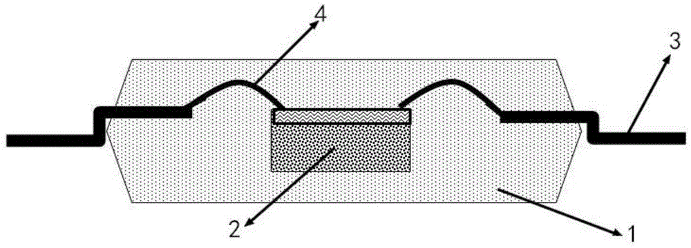
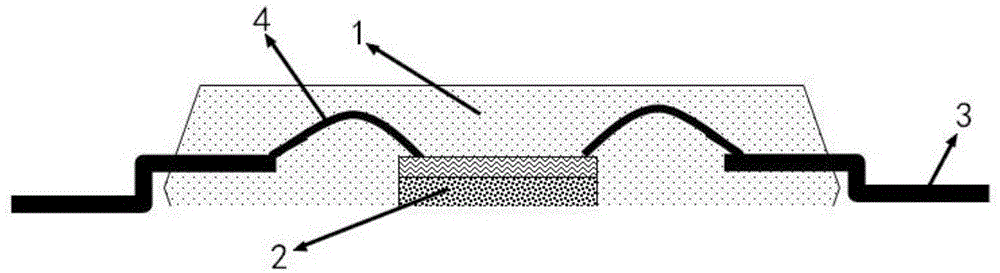
[0026] The first step is to select a sample chip and grind the sample chip from the back side. If it is a bare chip, first package the chip; if it is a packaged chip, it can be used directly, see figure 1 As shown in the figure, 1 is the package body, 2 is the chip, 3 is the pin, and 4 is the connecting wire. Grinding is carried out from the back of the package body 1, and according to the thickness of the chip, 5-200 μm is roughly ground first, leaving about 2-20 μm. like figure 2 .

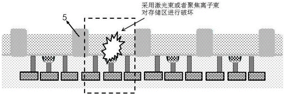
[0027] In the second step, the chemical etching method is used to continue etching the back surface until the insulating isolation layer 5 is exposed, such as image 3 . Some isolation layers are LOCOS (Local Oxide Layer) and some are STI (Shallow Trench Isolation). The purpose of exposing the insulating layer is to determine the location of the memory and the optio...


PUM


Abstract

The invention discloses a memory chip scrambling verification method which comprises the following steps: 1, selecting a packaged sample chip, and grinding the sample chip from the back according to the thickness of the chip; 2, continuously carrying out corrosion on the back of the sample chip by adopting a chemical corrosion way; 3, carrying out physical damage on the memory area and recording the physical address of the physical damage; 4, adding a protective cover on the back of the sample chip, transferring the sample chip onto a manual testing mechanism and manually testing; 5, selecting 2-20 sample chips, repeating the previous steps, testing different positions of the memory areas of all the sample chips to find out the failure electric address, and calculating the corresponding relation between the physical address and the electric address according to the physical address obtained in the step 3.

Description

technical field [0001] The invention relates to the field of integrated circuit failure analysis, in particular to a memory chip scrambling code verification method. Background technique [0002] For memory chips, whether it is a volatile memory or a non-volatile memory, during the manufacturing and use stages, failure modes such as single bit, multiple bits, entire row of bits, and entire column of bits may be encountered, affecting mass production and terminals. customer use. To find the root cause of the failure, it is necessary to perform a physical failure analysis on the chip, that is, to find out the actual physical address of the failed bit on the chip, and conduct a targeted physical dissection to find the root cause of the failure. [0003] For the physical dissection of the memory chip, it is generally necessary to perform scrambling code verification first, that is, to find out the correspondence between the electrical address and the physical address. The trad...

Claims


Application Information

Patent Timeline
Patent Type & Authority Applications(China)
IPC IPC(8): G11C29/56
Inventor 马香柏
Owner SHANGHAI HUAHONG GRACE SEMICON MFG CORP
Why Eureka
Try Eureka