Array substrate, manufacturing method thereof, and display device
A technology for array substrates and manufacturing methods, which is applied in semiconductor/solid-state device manufacturing, semiconductor/solid-state device components, semiconductor devices, etc., and can solve problems such as crystallization, increased complexity of the array substrate manufacturing process, and inability to etch, Achieve the effect of simplifying the manufacturing steps and preventing electrochemical corrosion
- Summary
- Abstract
- Description
- Claims
- Application Information
AI Technical Summary
Problems solved by technology
Method used
Image

Examples
Embodiment 1
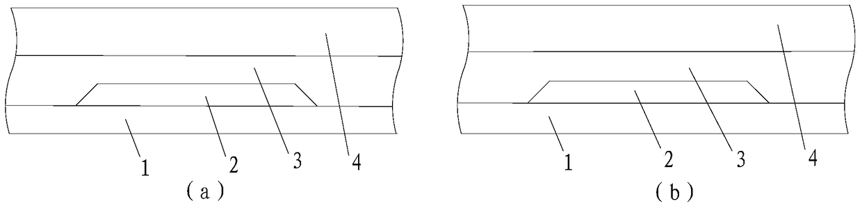
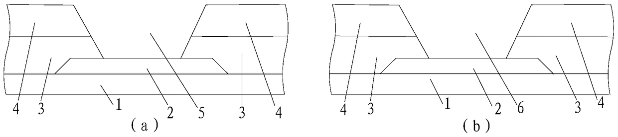
[0033] This embodiment provides a method for fabricating an array substrate, such as Figure 1 to Figure 8 As shown, the method includes the following steps:
[0034] Step S1: forming a plurality of first via holes 5 and a plurality of second via holes 6 on the substrate 1 on which the thin film transistors have been manufactured.
[0035] Step S2: covering the transparent conductive layer 7 on the substrate 1 after the first via hole 5 and the second via hole 6 are formed.
[0036] Step S3 : covering the transparent conductive layer 7 with a protective material layer 8 , the film forming temperature of the protective material layer is lower than the annealing temperature of the transparent conductive layer 7 .
[0037] Step S4: Forming the first electrode 12 covering the first via hole 5 and its surroundings, the second electrode 13 covering the second via hole 6 and its surroundings, and the first protective layer 10 covering the first electrode 12 by one patterning process ...
Embodiment 2
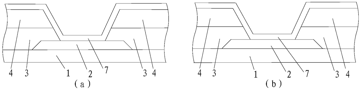
[0063] This embodiment provides an array substrate, including: a substrate and a thin film transistor on the substrate, such as Figure 8 As shown, the array substrate also includes: a plurality of first via holes and a plurality of second via holes arranged on the substrate 1; a first electrode 12 covering the first via holes and their surroundings; a second electrode covering the first electrode 12 A protective layer 10; covering the second via hole and the second electrode 13 around it. Wherein, the film forming temperature of the first protection layer 10 is lower than the annealing temperature of the first electrode 12 and the second electrode 13, and the first protection layer 10, the first electrode 12 and the second electrode 13 are formed in the same patterning process.
[0064] Since the first electrode 12 is covered with the first protective layer 10, the first protective layer 10 can protect the first electrode 12, effectively preventing the electrochemical corrosi...
Embodiment 3
[0069] This embodiment provides a display device, including the array substrate described in the second embodiment. Since the array substrate described in Embodiment 2 can protect the first electrode 12 by using the first protection layer 10 on the premise of saving the number of patterning processes and simplifying the manufacturing steps, so as to prevent the first electrode 12 from deteriorating, the The provided display device also has the advantage of preventing the deterioration of the first electrode 12 under the premise of saving the number of patterning processes and simplifying the manufacturing steps, and has higher reliability and display quality.
[0070] It should be noted that the display device provided in this embodiment can be a liquid crystal panel, electronic paper, OLED (Organic Light-Emitting Diode, organic light-emitting diode) panel, mobile phone, tablet computer, television, monitor, notebook computer, digital photo frame , navigator and any other prod...
PUM
 Abstract
Description
Claims
Application Information
 - R&D
- Intellectual Property
- Life Sciences
- Materials
- Tech Scout
- Unparalleled Data Quality
- Higher Quality Content
- 60% Fewer Hallucinations
Browse by: Latest US Patents, China's latest patents, Technical Efficacy Thesaurus, Application Domain, Technology Topic, Popular Technical Reports.
© 2025 PatSnap. All rights reserved.Legal|Privacy policy|Modern Slavery Act Transparency Statement|Sitemap|About US| Contact US: help@patsnap.com