Inductor in three-dimensional stack package chip and its preparation method
A technology of three-dimensional stacking and mounting chips, which is applied in the direction of circuits, electrical components, and electrical solid devices, can solve the problems of low inductance, limited inductance size, and inability to meet high inductance and high Q value, etc., to increase the chip plane area, the effect of increasing the inductance value
- Summary
- Abstract
- Description
- Claims
- Application Information
AI Technical Summary
Problems solved by technology
Method used
Image


Examples
preparation example Construction
[0041] According to the core idea of the present invention, a preparation method is also provided, such as figure 1 shown, including:
[0042] Step S11 : providing a first wafer, including a first substrate and a first dielectric layer on one side of the first substrate, a first inductor is formed in the first dielectric layer, and the first dielectric layer A first conductive plug is provided on a side away from the first substrate, and the first conductive plug is connected to the first inductor;
[0043] Step S12 : providing a second wafer, including a second substrate and a second dielectric layer on one side of the second substrate, a second inductor is formed in the second dielectric layer, and the second dielectric layer A side away from the second substrate is provided with a second conductive plug, the second conductive plug is connected to the second inductor;
[0044] Step S13 : bonding the first wafer and the second wafer together, wherein the side of the first d...
no. 1 example
[0047] below, see Figure 2-Figure 4 The inductor in the three-dimensional stacked package chip of the present invention and its manufacturing method are specifically described. In this embodiment, the inductor consists of two stacked sub-inductors, and the two sub-inductors are located in two stacked wafers respectively.
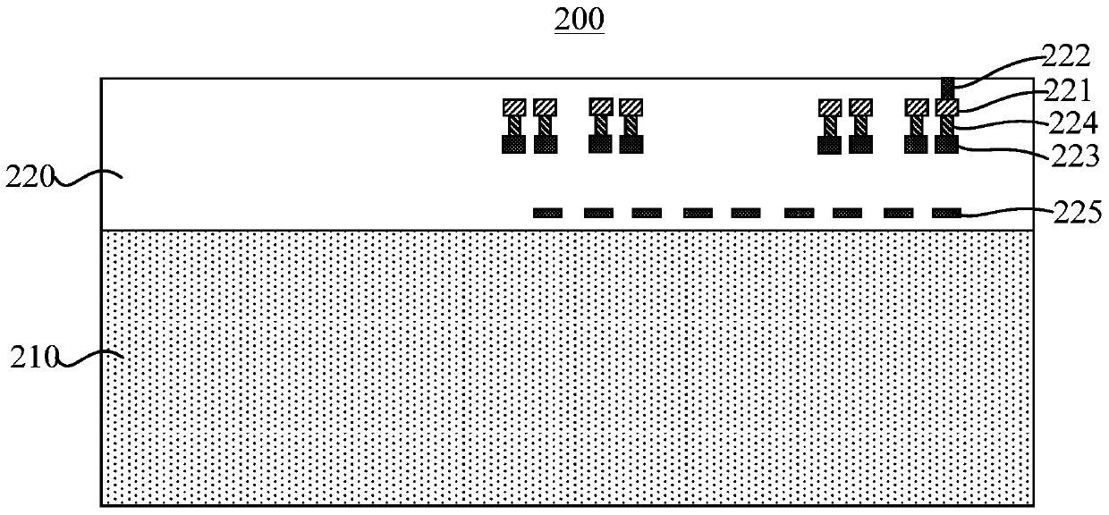
[0048] First, as figure 2 As shown, step S11 is performed to provide a first wafer 100 . The first wafer 100 includes a first substrate 110 and a first dielectric layer 120 located on one side of the first substrate 110 . The thickness of the first substrate 110 is generally thick, about 500 μm˜800 μm, such as 500 μm, 600 μm, 700 μm, etc. The material of the first dielectric layer 120 is generally oxide. A first inductor 121 is formed in the first dielectric layer, wherein the first wafer 100 is formed by an integrated circuit process, and the first dielectric layer 120 and the first inductor 121 pass through the BEOL (after The specific interconnection ...
no. 2 example
[0058] see Figure 5-Figure 10 , Figure 5-Figure 10 It is a schematic cross-sectional view of the chip in the manufacturing process of the inductor in the three-dimensional stacked package chip according to the second embodiment of the present invention. The inductor 2 of the second embodiment is basically the same as the inductor 1 of the first embodiment, and the difference is that after step S13, it further includes:
[0059] like Image 6 As shown, the side of the first substrate 110 away from the first dielectric layer 120 is thinned, and the thickness of the first substrate 110 is reduced to 2 μm˜5 μm, which is beneficial to the preparation of the third conductive plug .
[0060] Then, as in Figure 7 As shown, an opening 126 is formed on the first substrate 110 away from the first dielectric layer 120, such as Figure 8 As shown, the openings 126 are filled with conductive materials to form third conductive plugs 127 . In this embodiment, the third conductive plu...
PUM
 Abstract
Description
Claims
Application Information
 - R&D
- Intellectual Property
- Life Sciences
- Materials
- Tech Scout
- Unparalleled Data Quality
- Higher Quality Content
- 60% Fewer Hallucinations
Browse by: Latest US Patents, China's latest patents, Technical Efficacy Thesaurus, Application Domain, Technology Topic, Popular Technical Reports.
© 2025 PatSnap. All rights reserved.Legal|Privacy policy|Modern Slavery Act Transparency Statement|Sitemap|About US| Contact US: help@patsnap.com