Oxide film transistor and manufacturing method thereof

A technology of oxide thin film and manufacturing method, which is applied in transistors, semiconductor/solid-state device manufacturing, electric solid-state devices and other directions, can solve problems such as the influence of oxide thin-film transistor characteristics, the normal use of thin-film transistors, and the damage to the back channel, etc. Save production time, save production cost, and improve the effect of features

Inactive Publication Date: 2015-05-13
TCL CHINA STAR OPTOELECTRONICS TECH CO LTD
View PDF6 Cites 17 Cited by
  • Summary
  • Abstract
  • Description
  • Claims
  • Application Information

AI Technical Summary

Problems solved by technology

However, it is easy to cause damage to the back channel when etching the source / drain electrodes or depositing a passivation layer. For example, if dry etching is used, when the source and drain electrodes are formed by dry etching, the plasma formed by the etching gas will Bombard the back channel, and the plasma bombardment will cause more defects in the back channel, which will affect the normal use of the thin film transistor; if wet etching is used, when the source and drain electrodes are formed by wet etching, the etchant will have a negative effect. Corrosion of the source layer oxide will damage the back channel, and the characteristics of the oxide thin film transistor will be affected

Method used


Image

  • Oxide film transistor and manufacturing method thereof
  • Oxide film transistor and manufacturing method thereof

Examples


Embodiment Construction

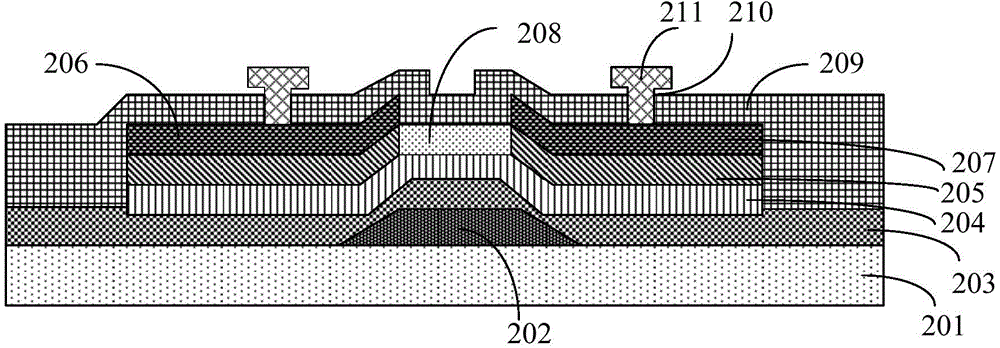
[0031] refer to figure 1 , figure 1 It is a schematic flowchart of an embodiment of the method for fabricating an oxide thin film transistor of the present invention. The manufacturing method of the present embodiment comprises the following steps:

[0032] 101: Form a gate, a gate insulating layer, and an oxide semiconductor film layer sequentially on a first substrate.

[0033] Specifically, firstly, a metal film layer is formed on the first substrate by deposition, the metal film layer is exposed through a first photomask, and the metal film layer is etched to form a gate. Among them, the first photomask is an ordinary photomask that can only etch one layer.

[0034] Wherein, the first substrate includes a glass substrate and a quartz substrate, and may also be other substrates in other implementation manners, which is not limited here.

[0035] The metal film layer includes at least one of aluminum Al, molybdenum Mo, copper Cu, and silver Ag, and may be other metals in...


PUM

PropertyMeasurementUnit
thicknessaaaaaaaaaa

Abstract

The invention discloses an oxide film transistor and a manufacturing method thereof. The manufacturing method comprises sequentially forming a grid electrode, a grid electrode insulating layer and an oxide semiconductor film layer; sequentially forming a first metal layer and a second metal layer on the oxide semiconductor film layer, and forming a drain electrode and a source electrode on the second metal layer, wherein the source electrode and the drain electrode are separated through a channel which exposes a part of the first metal layer; oxidizing the exposed part of first metal layer; forming an insulating passivation layer and setting a contact electrode. The manufacturing method of the oxide film transistor can protect the back channel of the oxide film transistor and meanwhile simplify the manufacturing process and save the cost.

Description

technical field [0001] The invention relates to the field of field display, in particular to an oxide thin film transistor and a manufacturing method thereof. Background technique [0002] With the development of flat panel displays represented by liquid crystal LCDs and organic light emitting diodes (OLEDs) toward large size and high resolution, thin-film transistors (TFTs), as the core components of the flat panel display industry, have also received widespread attention. [0003] Commonly used thin film transistors in the prior art include amorphous silicon thin film transistors and oxide thin film transistors. Oxide thin film transistors have the advantages of high carrier mobility, and there is no need to greatly change the existing liquid crystal panel production lines when they are introduced. And has been widely used. [0004] The oxide thin film transistor includes two structures of top gate and bottom gate, and the bottom gate structure mainly adopts two structure...

Claims


Application Information

Patent Timeline
Patent Type & Authority Applications(China)
IPC IPC(8): H01L29/786H01L21/34
CPCH01L21/34H01L29/786H01L29/7869H01L29/40114H01L27/12H01L29/66969H01L27/1288H01L23/3171H01L29/4908H01L29/4966H01L29/518
Inventor 迟世鹏
Owner TCL CHINA STAR OPTOELECTRONICS TECH CO LTD
Why Eureka
Try Eureka