Backside illuminated CMOS sensor and preparation method thereof

A CMOS sensor and back-illuminated technology, which is applied in the field of back-illuminated CMOS sensors and the preparation of the sensor, can solve the problems that the quantum conversion efficiency of the sensor needs to be improved, and achieve the effect of improving the quantum conversion efficiency

Inactive Publication Date: 2015-04-29
OMNIVISION TECH (SHANGHAI) CO LTD
View PDF11 Cites 3 Cited by
  • Summary
  • Abstract
  • Description
  • Claims
  • Application Information

AI Technical Summary

Problems solved by technology

[0008] In view of the above existing problems, the present invention discloses a back-illuminated CMOS sensor and a method for preparing the sensor, so as to solve the problem that the quantum conversion efficiency of the back-illuminated CMOS sensor needs to be improved in the prior art

Method used


Image

  • Backside illuminated CMOS sensor and preparation method thereof
  • Backside illuminated CMOS sensor and preparation method thereof
  • Backside illuminated CMOS sensor and preparation method thereof

Examples


Embodiment 1

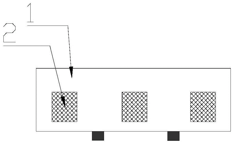
[0038] Figure 6 It is a structural schematic diagram of a back-illuminated CMOS sensor in an embodiment of the present invention; as Figure 6 As shown, a back-illuminated CMOS sensor (BSI CMOS sensor), the sensor includes a wafer 1 with several photodiodes 2 and a dielectric layer 3 arranged on the front of the wafer 1, and the dielectric layer 3 is close to the wafer 1 A groove 4 is provided at the position and the groove 4 is located below the photodiode 2, and a light-reflecting material is arranged in the groove 4, wherein the groove 4 is a rectangular structure, and its width is greater than that of the photodiode 2, and the dielectric layer 3 is also provided with a There are through holes 5 and metal interconnection lines 6, one end of the through hole 5 is connected to the electrode of the wafer 1, and the other end is connected to the metal interconnection line 6, metal is provided in the through hole 5, and a wafer substrate 11 is located on the wafer 1, the optic...

Embodiment 2

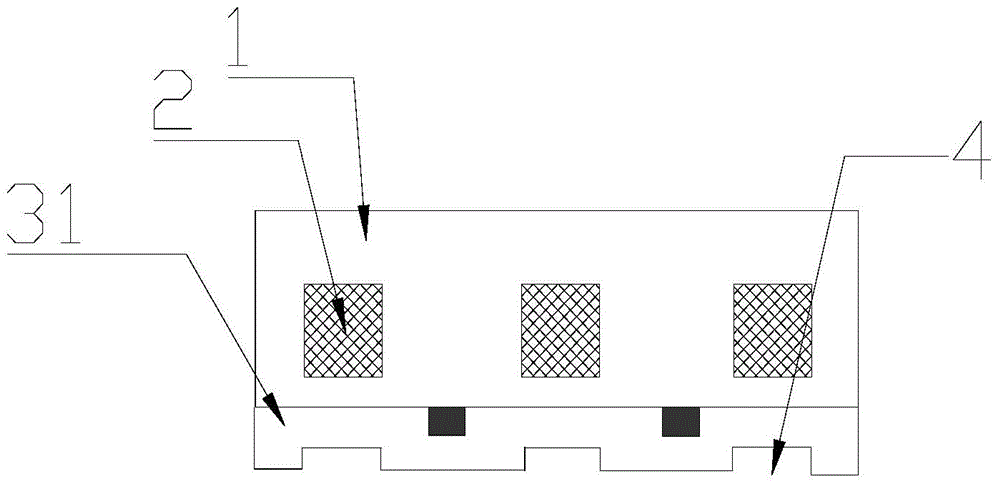
[0043] Figure 1~5 It is a schematic flow chart of the method for preparing a back-illuminated CMOS sensor in an embodiment of the present invention, Figure 6 is a schematic structural diagram of a back-illuminated CMOS sensor in an embodiment of the present invention, such as Figure 1~6 Shown:

[0044] First provide a wafer 1 with several photodiodes 2, such as figure 1 the structure shown;

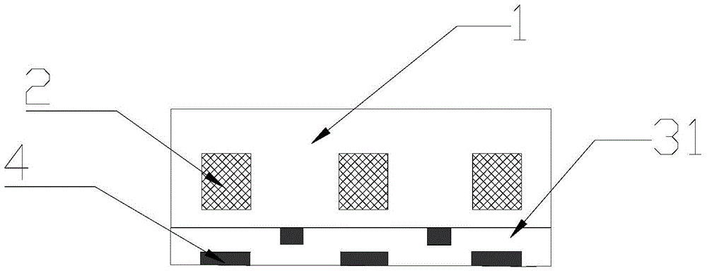
[0045] Next, deposit a first dielectric layer 31 on the front of the wafer 1, and etch the first dielectric layer 31 below the photodiode 2 to form a trench 4, which can be dry-etched or wet-etched, and the trench 4 has a rectangular structure, and width is greater than the width of the photodiode, as figure 2 the structure shown;

[0046]Then, deposit a reflective substance such as aluminum or tungsten on the groove 4, and perform polishing, which can be polished by chemical mechanical polishing (CMP), such as image 3 the structure shown;

[0047] Then, deposit the second die...


PUM


Abstract

The invention discloses a backside illuminated CMOS sensor and a preparation method thereof. The backside illuminated CMOS sensor comprises a wafer, a dielectric layer arranged on the front surface of the wafer, a groove arranged in the dielectric layer and close to the wafer, and a through hole and a metal interconnecting wire which are arranged in the dielectric layer, wherein a plurality of photodiodes are formed in the wafer; the groove is positioned below the photodiodes; light reflecting substance is arranged in the groove; one end of the through hole is connected with the electrode of the wafer; the other end of the through hole is connected with the metal interconnecting wire; metal is arranged in the through hole. The backside illuminated CMOS sensor improves the quantum conversion efficiency, further improves the product image quality, is higher in compatibility than that of the traditional processing equipment, and is simple and practicable in technology.

Description

technical field [0001] The invention relates to the field of semiconductor manufacturing, in particular to a back-illuminated CMOS sensor and a method for preparing the sensor. Background technique [0002] Because CMOS sensors have high image acquisition speed and high anti-interference, they also have the characteristics of low operating voltage and low power consumption, and can use the same high-capacity wafer production line to prepare CMOS image sensors, making CMOS sensors It has been developed rapidly and widely used in production and life. [0003] The back-illuminated CMOS sensor (BSI CMOS sensor) turns the direction of the original photosensitive layer so that the light enters directly from the back of the device, thus effectively avoiding the traditional CMOS sensor structure, where the light needs to pass between the microlens and the photodiode. Only the circuit, transistor and other structural layers can reach the photosensitive layer, which greatly improves ...

Claims


Application Information

Patent Timeline
Patent Type & Authority Applications(China)
IPC IPC(8): H01L27/146
Inventor 高喜峰邢家明
Owner OMNIVISION TECH (SHANGHAI) CO LTD
Why Eureka
Try Eureka