Power semiconductor module and method for producing a power semiconductor module

一种功率半导体、导通的技术,应用在半导体/固态器件制造、半导体器件、半导体/固态器件零部件等方向,能够解决绝缘层昂贵等问题

Active Publication Date: 2017-07-14
INFINEON TECH AG
View PDF5 Cites 0 Cited by
  • Summary
  • Abstract
  • Description
  • Claims
  • Application Information

AI Technical Summary

Problems solved by technology

[0004] Of course, this method requires an additional insulating layer through which the chip housings must be covered, which creates an additional operating step
In addition, it can only be expensive to realize the production of insulating layers under the integrated circuit.

Method used


Image

  • Power semiconductor module and method for producing a power semiconductor module
  • Power semiconductor module and method for producing a power semiconductor module
  • Power semiconductor module and method for producing a power semiconductor module

Examples


Embodiment Construction

[0016] In the figures, the same reference numerals designate the same components or signals with the same or similar meanings.

[0017] In the description set forth below, reference is made to the accompanying drawings, in which a number of specific exemplary embodiments are shown for illustration purposes. Unless stated otherwise, the symbols of the different exemplary embodiments described here can of course be combined with one another.

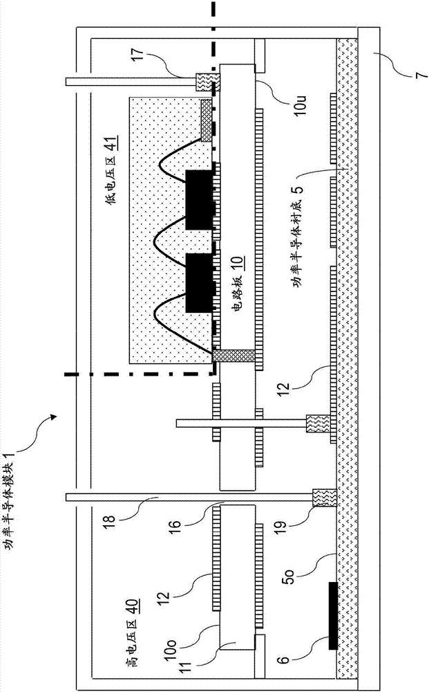
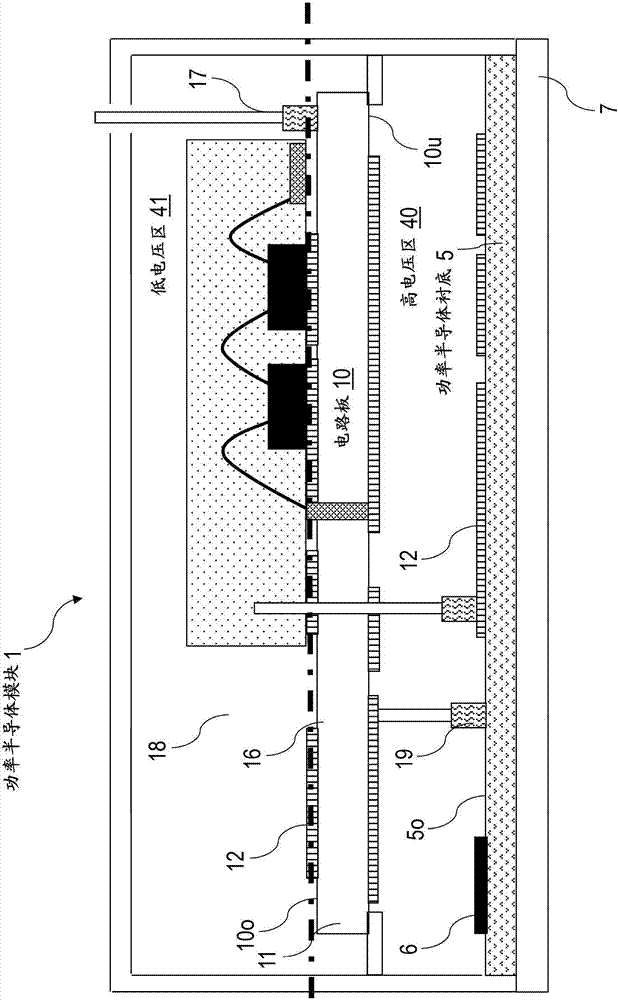
[0018] Figure 1A A sectional view through a power semiconductor module 1 according to an example of the invention is shown. The specific design of the control circuit board 10 makes it possible to integrate not only the power electronics components but also the control electronics in a compact housing (eg Infineon's 2B), which has hitherto only accommodated power electronics components (excluding control circuit boards). The circuit board 10 and the power semiconductor substrate 5 are arranged one above the other in the example shown i...


PUM


Abstract

The invention relates to a power semiconductor module. According to one example of the invention, the power semiconductor module has a circuit board with a structured first metal structure and at least one second metal structure arranged on the upper side of the circuit board. At least one housingless semiconductor chip is arranged on the top side of the circuit board, the semiconductor chip has a plurality of contact electrodes, which in turn are connected to corresponding contact pads of the first metal structure on the top side of the circuit board via bonding wires connect. During operation, the contact electrodes and the corresponding first part of the contact lugs are connected to a high voltage. All high-voltage-connected contact lugs are electrically conductively connected to the second metal structure via inner-layer connections. The insulating layer completely covers the chip and the separation area of ​​the circuit board surrounding the chip, wherein all contact pads and inner layer connections for high-voltage switching are completely covered by the insulating layer. The plurality of contact electrodes and the corresponding second portion of the contact pads are at a low voltage during operation.

Description

technical field [0001] The invention relates to the field of power semiconductor modules, their construction and production methods. Background technique [0002] Modern power semiconductor modules comprise integrated circuits (ICs) as main components in addition to power electronic semiconductor components (in particular power semiconductor switches). It is used, for example, to switch on power semiconductor switches or to measure current or temperature. In this case it is often referred to as an "Intelligent Power Semiconductor Module" ("Intelligent Power Module", abbreviation: IPM). Such an IPM includes a drive circuit (gate driver) etc. that are usually added to a power electronic device. Common operating voltages in power semiconductor modules can range from hundreds of volts to thousands of volts. These high voltages are applied to the external contacts (high voltage contacts) of integrated circuits (eg gate drivers), so effective insulation is required for these in...

Claims


Application Information

Patent Timeline
Patent Type & Authority Patents(China)
IPC IPC(8): H01L25/16H01L23/498H01L23/055H01L21/60
CPCH01L2224/48091H01L2224/48137H05K1/0256H05K1/144H05K3/28H05K3/284H05K2201/042H05K2201/10303H05K2201/10318H01L2924/13055H01L2924/181H01L23/3121H01L2224/48227H05K7/14322H01L2924/00014H01L2924/00H01L2924/00012H05K7/1432H01L21/56H01L25/18H01L25/50H05K1/111H05K1/181H05K2201/0104
Inventor A·阿伦斯J·赫格尔M·霍伊
Owner INFINEON TECH AG
Why Eureka
Try Eureka