
On-chip switch step-by-step control circuit and method, on-chip signal pin drive circuit

A step-by-step control and switching tube technology, applied in the direction of electronic switches, electrical components, pulse technology, etc., can solve the problem of increasing the time of the turn-on or turn-off process, unable to reduce the interference of self-induced electromotive force, and unable to effectively reduce the current change rate and other problems, to achieve the effect of shortening the switching process time, reducing the current change rate, and speeding up

Active Publication Date: 2017-12-26
VERISILICON MICROELECTRONICS SHANGHAI +3
View PDF9 Cites 0 Cited by
  • Summary
  • Abstract
  • Description
  • Claims
  • Application Information

AI Technical Summary

Problems solved by technology

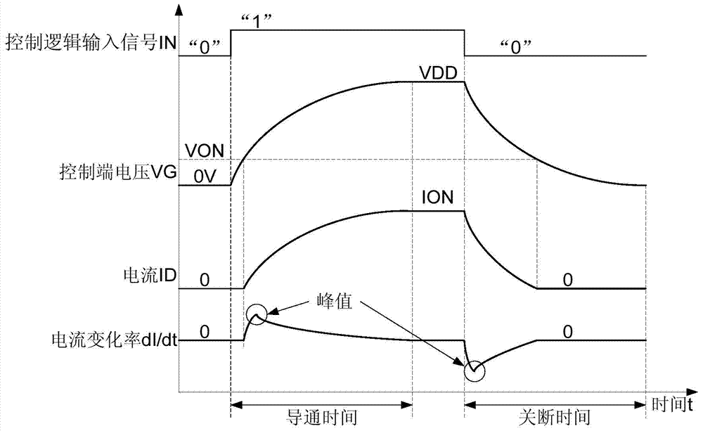
[0010] In view of the shortcomings of the prior art described above, the purpose of the present invention is to provide an on-chip switch step-by-step control circuit and method, and an on-chip signal pin drive circuit, which are used to solve the problem that the current rate of change cannot be effectively reduced in the prior art, thereby It cannot reduce the interference of self-inductance electromotive force, but increases the time of the turn-on or turn-off process, resulting in the problem of reduced switching speed

Method used


Image

  • On-chip switch step-by-step control circuit and method, on-chip signal pin drive circuit
  • On-chip switch step-by-step control circuit and method, on-chip signal pin drive circuit
  • On-chip switch step-by-step control circuit and method, on-chip signal pin drive circuit

Examples


Embodiment Construction

[0079] Embodiments of the present invention are described below through specific examples, and those skilled in the art can easily understand other advantages and effects of the present invention from the content disclosed in this specification. The present invention can also be implemented or applied through other different specific implementation modes, and various modifications or changes can be made to the details in this specification based on different viewpoints and applications without departing from the spirit of the present invention.

[0080] see Figure 4 , The first embodiment of the present invention relates to an on-chip switch step-by-step control circuit. It should be noted that the diagrams provided in this embodiment are only schematically illustrating the basic idea of ​​the present invention, and only the components related to the present invention are shown in the diagrams rather than the number, shape and shape of the components in actual implementation....


PUM


Abstract

The present invention provides an on-chip switch step-by-step control circuit and method, and an on-chip signal pin drive circuit. The on-chip switch step-by-step control circuit at least includes: a switch tube module, and the switch tube module includes at least n stages of switch tubes connected in parallel. The control terminal drive module, the control terminal drive module at least includes n-level drivers, and the output terminals of the drivers at all levels are connected to the control terminals of the switch tubes at all levels respectively, and are used to drive the switch tubes at all levels; the delay chain, the delay chain The time chain includes at least n-1 delay modules connected in series, wherein the input end of the first-stage delay module and the input end of the first-stage driver are jointly connected to a control logic input signal, and the n-1th stage delay The output terminal of the module is connected with the input terminal of the nth level driver. The on-chip switch step-by-step control circuit of the present invention can effectively reduce the current change rate, and has the shortest turn-on or turn-off process on the premise of reducing the current change rate, so that the switch speed can be maximized.

Description

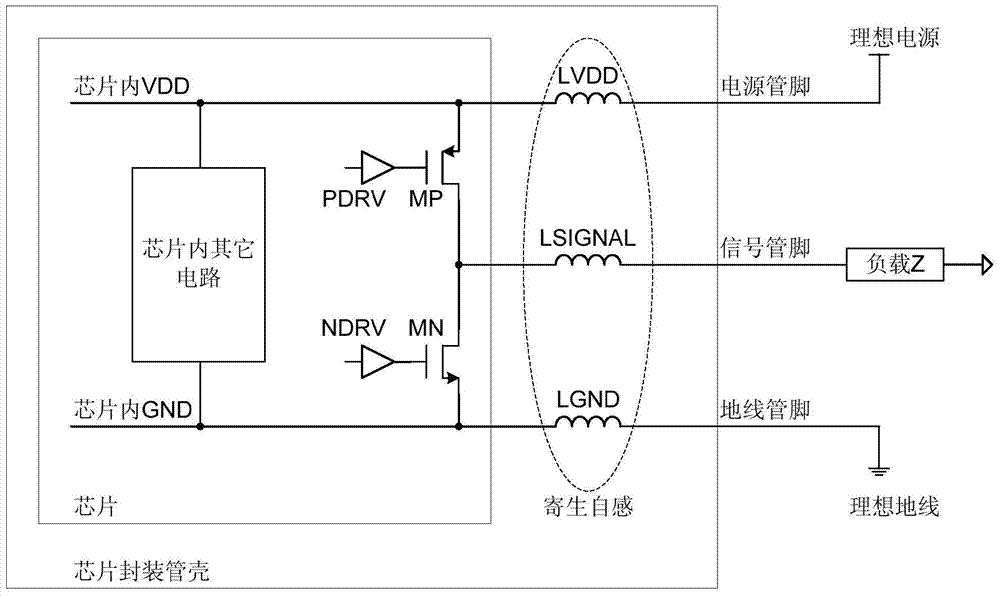
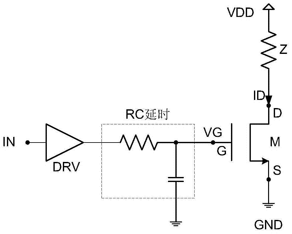
technical field [0001] The invention relates to the technical field of large-scale integrated circuit design, in particular to an on-chip switch step-by-step control circuit and method, and an on-chip signal pin drive circuit. Background technique [0002] With the improvement of the integration level of modern chips, more and more signal pins need to be driven on the same chip. The loads to be driven by these signal pins may be different. For example, ordinary CMOS digital signal pins drive capacitors, switching power supply signal pins drive inductors, and high-speed interface DDR signal pins drive transmission lines with resistive loads. But no matter what kind of load it is, the essential function of the output stage switch control circuit is to quickly switch the current between the signal pin and the power line or ground line. And all these current switches will face a common problem, which is the disturbance to the power line (or ground line) in the chip. [0003] S...

Claims


Application Information

Patent Timeline
Patent Type & Authority Patents(China)
IPC IPC(8): H03K17/28H03K17/08H03K17/687
Inventor 张武全陈立新费伟斌
Owner VERISILICON MICROELECTRONICS SHANGHAI
Learn More