Method of forming through silicon vias

A technology of TSV and laser, applied in electrical components, semiconductor/solid-state device manufacturing, circuits, etc., can solve the problems of easy metal copper layer diffusion, affecting the reliability of TSV, poor contact between TSV and metal layer, etc. , to achieve the effect of high absorbance and efficient homogenization treatment

Active Publication Date: 2017-11-03
SEMICON MFG INT (SHANGHAI) CORP
View PDF5 Cites 0 Cited by
  • Summary
  • Abstract
  • Description
  • Claims
  • Application Information

AI Technical Summary

Problems solved by technology

However, due to technological reasons, during the formation of through-silicon vias, after the metal copper layer filled in the through-holes is planarized, the periphery of the upper surface will be damaged, resulting in surface pitting in the through-silicon vias.
Once there is a surface gap in the TSV, the subsequent formation of the metal layer on the TSV may cause poor contact between the TSV and the metal layer on the one hand, thereby reducing the conductivity of the TSV, and on the other hand, it may cause easy metallization. Diffusion of the copper layer affects the reliability of TSVs and affects production efficiency
[0005] For this reason, a new method for forming through-silicon vias is needed to solve the problem of surface gaps in existing through-silicon vias

Method used


Image

  • Method of forming through silicon vias
  • Method of forming through silicon vias
  • Method of forming through silicon vias

Examples


Embodiment Construction

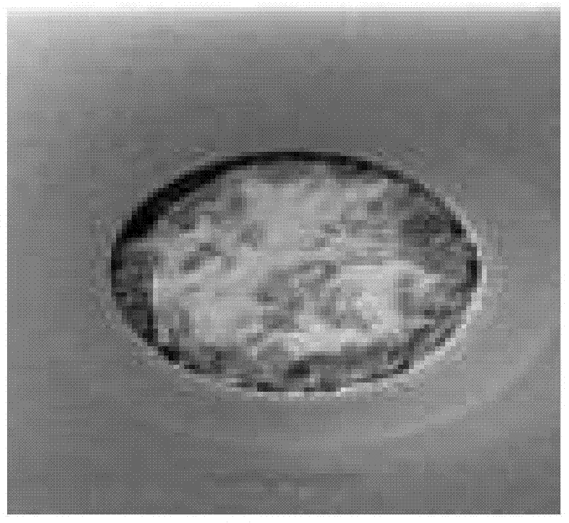
[0024] Through-silicon vias are prone to surface notches. It is found through inspection that the TSVs located in the central area of ​​the wafer surface are different from the TSVs located in the edge area of ​​the wafer surface. Please refer to figure 1 with figure 2 , figure 1 The scanning electron microscope image in shows the surface gap of the TSV located in the central area of ​​the wafer surface, while the figure 2 The scanning electron microscope image in shows surface notches in the TSVs located in the edge region of the wafer surface.

[0025] There are two main reasons for the existence of surface gaps in TSVs.

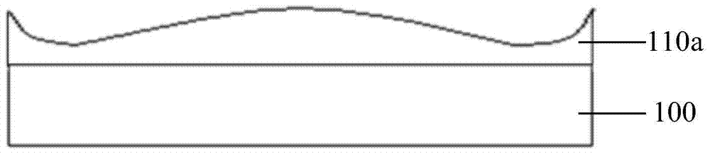
[0026] The first point is that for the entire wafer, during the electroplating metal copper layer process, the thickness of the metal copper layer deposited on the central area of ​​the wafer surface and the edge area of ​​the wafer surface are different. Such as image 3 As shown, the thickness of the metal copper layer 110a at the center of the su...


PUM

PropertyMeasurementUnit
wavelengthaaaaaaaaaa

Abstract

The invention provides a method for forming a through silicon via. The method for forming the through silicon via includes the steps that a wafer is provided; the through silicon via is formed in the wafer; an insulating layer is formed on the surface of the through silicon via; metallic copper layers are arranged in the through silicon via and on the upper surface of the wafer; the surfaces of the metallic copper layers are homogenized through laser thermal annealing; the metallic copper layers are flattened till the surface of the wafer is exposed. By the adoption of the method for forming the through silicon via, the surface of the formed through silicon via is flat, and the conductivity and the reliability of the formed through silicon via are improved.

Description

technical field [0001] The invention relates to the technical field of semiconductors, in particular to a method for forming through-silicon holes. Background technique [0002] With the continuous development of semiconductor technology, the feature size of semiconductor devices has become very small. It is becoming more and more difficult to increase the number of semiconductor devices in a two-dimensional packaging structure. Therefore, three-dimensional packaging has become a method that can effectively improve chip integration. degree method. Current three-dimensional packaging includes die stacking based on wire bonding, package stacking and three-dimensional stacking based on through silicon vias (Through Silicon Via, TSV). [0003] The three-dimensional stacking technology based on through-silicon vias has the following three advantages: (1) high-density integration; (2) greatly shortening the length of electrical interconnections, which can well solve the problems ...

Claims


Application Information

Patent Timeline
Patent Type & Authority Patents(China)
IPC IPC(8): H01L21/768
CPCH01L21/268H01L21/768
Inventor 沈哲敏赵洪波何作鹏
Owner SEMICON MFG INT (SHANGHAI) CORP
Why Eureka
Try Eureka