Method for preparing ONO medium layer

A dielectric layer and bottom layer technology, which is applied in semiconductor/solid-state device manufacturing, electrical components, semiconductor devices, etc., can solve problems such as uneven distribution, intensified gas distribution, and influence on electrical uniformity, so as to achieve strong realizability and reduce shell Body, improve the effect of thickness uniformity

Active Publication Date: 2015-03-25
SHANGHAI HUALI MICROELECTRONICS CORP
View PDF6 Cites 2 Cited by
  • Summary
  • Abstract
  • Description
  • Claims
  • Application Information

AI Technical Summary

Problems solved by technology

[0007] However, during the preparation process of the ONO dielectric layer, the technicians found some problems. When the tooth spacing in the crystal boat box is 8mm to 11mm, the silicon wafers 15 in the wafer boat box 12 are distributed in a trapezoidal shape, and the upper and lower adjacent two The distances at each position of the silicon wafer 15 are equal, causing the reaction gas concentration at the center position of the upper surface of the silicon wafer 15 to be lower than the gas concentration at the edge position, thereby causing the thickness of the oxide film grown at the edge position of the upper surface of the silicon wafer to be the same as that on the silicon wafer. There is a large difference in the thickness of the oxide film grown at the center of the surface
[0008] image 3 It is a schematic diagram of the gas flow state after the reaction gas is introduced into the reaction furnace in the prior art. As can be seen from the figure, the gas is not easy to flow to the center of the silicon wafer 15 during the flow process, and the concentration is relatively high at the edge of the silicon wafer, resulting in The thickness of the film in the middle of the silicon wafer is thinner than that of the edge of the silicon wafer. After the stacked ONO interlayer dielectric is deposited with three layers of LPCVD films, the thickness difference on the silicon wafer will be enlarged, and the edge is thicker and the middle is thinner. At the same time, in the traditional process of ONO In the preparation process, when preparing the intermediate silicon nitride, the general technical solution is to directly feed the gas used for the preparation of silicon nitride at the same time to react to form silicon nitride covering the bottom silicon oxide, but in the reaction process In the process, the distribution of nitrogen-containing gas and silicon-containing gas in the reaction furnace is uneven, and at the same time, due to the circulation of gas in the reaction furnace such as image 3 As shown, the phenomenon of uneven gas distribution is further exacerbated, thus resulting in uneven thickness of silicon nitride formed on the surface of the silicon wafer
The unevenness of the thickness will affect the uniformity of the electrical properties, which will cause differences in the reading and writing speeds and data retention capabilities of different positions

Method used


Image

  • Method for preparing ONO medium layer
  • Method for preparing ONO medium layer
  • Method for preparing ONO medium layer

Examples


Embodiment Construction

[0036] In the following description, a lot of specific details are given in order to provide a more thorough understanding of the present invention. However, it is obvious to those skilled in the art that the present invention can be implemented without one or more of these details. In other examples, in order to avoid confusion with the present invention, some technical features known in the art are not described.

[0037] In order to thoroughly understand the present invention, detailed steps and detailed structures will be presented in the following description to explain the technical solution of the present invention. The preferred embodiments of the present invention are described in detail as follows. However, in addition to these detailed descriptions, the present invention may also have other embodiments.

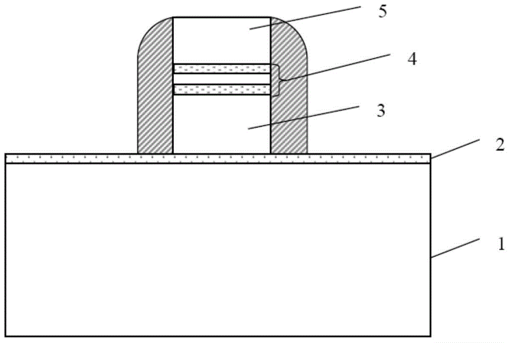
[0038] The present invention provides a method for preparing an ONO dielectric layer, including the following steps: A method for preparing an ONO dielectric layer, su...


PUM


Abstract

The invention relates to the field of semiconductor preparation, in particular to a method for preparing an ONO medium layer. The method is suitable for a nonvolatile NOR flash memorizer. The method includes the following steps of firstly, providing a silicon wafer, wherein a surface tunneling oxide layer and a floating gate layer formed at a preset position are sequentially arranged on a substrate of the silicon wafer; secondly, inputting first preset reaction gas through an in-situ vapor generation process, and forming bottom layer silicon oxide on the upper face of the floating gate layer; thirdly, inputting second preset reaction gas through a porous quartz tube, and forming silicon nitride on the upper side of the bottom layer silicon oxide through deposition; fourthly, inputting the first preset reaction gas through the in-situ vapor generation process, and oxidizing the surface of the silicon nitride to form top layer silicon oxide. The method has the advantages that the thickness uniformity of a thin film depositing on the surface of the silicon wafer is effectively improved, shells produced by the silicon wafer is remarkably reduced, N type dopes are not prone to being formed on contact faces of the silicon oxide and the silicon wafer, realizability is high, and the method can be widely applied to various deposition processes.

Description

Technical field [0001] The invention relates to the field of semiconductor preparation, in particular to a method for preparing an ONO dielectric layer. Background technique [0002] The stacked ONO structure is widely used in the chip manufacturing process. Used as an interlayer dielectric between the floating gate (FG) and the control gate (CG) in nonvolatile flash memory (NOR FLASH); it can also be used as a dynamic memory (Dynamic Random Access Memory) and a metal insulator (Metal Insulator). Insulator Metal, MIM) dielectric. [0003] The stacked gate is usually like figure 1 As shown, a tunnel oxide layer 2, a floating gate 3, an ONO (Oxide-Nitride-Oxide) dielectric layer 4, and a control gate 5 are sequentially formed on the substrate 1. [0004] When the stacked ONO structure is used as the interlayer dielectric between the floating gate and the control gate, the thickness uniformity of the three layers of ONO needs to be strictly controlled. When the overall thickness beco...

Claims


Application Information

Patent Timeline
Patent Type & Authority Applications(China)
IPC IPC(8): H01L21/28H01L21/285
CPCH01L21/28H01L21/285H01L29/40117H01L29/792
Inventor 江润峰孙天拓
Owner SHANGHAI HUALI MICROELECTRONICS CORP
Why Eureka
Try Eureka