PCB electrogilding technology

A PCB board and electro-gold technology, which is applied in the field of printed circuit boards, can solve the problems of waste of precious metals, increase production costs, and gold consumption, and achieve the effects of saving gold, reducing production costs, and reducing the area to be plated

Inactive Publication Date: 2015-03-11
深圳恒宝士线路板有限公司
View PDF18 Cites 7 Cited by
  • Summary
  • Abstract
  • Description
  • Claims
  • Application Information

AI Technical Summary

Problems solved by technology

[0003] In the traditional electro-gold process of printed circuit boards, all conductive patterns need to be plated with gold, so a large amount of gold is consumed, and electro-gold in parts that do not need electro-gold leads to waste of precious metals and greatly increases the cost of the enterprise. Cost of production

Method used


Image

  • PCB electrogilding technology
  • PCB electrogilding technology

Examples


Embodiment Construction

[0019] The following will clearly and completely describe the technical solutions in the embodiments of the present invention in conjunction with the accompanying drawings.

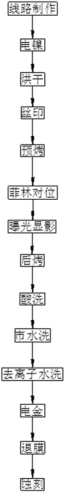
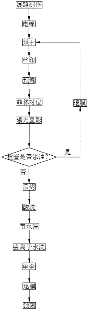
[0020] refer to figure 1 , the embodiment of the present invention provides a kind of PCB electro-gold process, comprising the following steps: circuit making: making circuit on the circuit board after copper plating; electro-nickel: electroplating nickel on the electro-nickel area of ​​the circuit board; drying : drying the circuit board after electro-nickel; silk screen printing: use photosensitive ink to carry out silk screen printing on the circuit board; pre-baking: pre-baking the circuit board after silk screen printing; Alignment; exposure and development: exposure and development of the film after alignment; post-baking: post-baking of the circuit board after exposure and development; pickling: pickling of the circuit board after post-baking; city water washing: pickling After the circuit board i...


PUM


Abstract

The invention discloses the PCB manufacturing technology. The PCB electrogilding technology comprises steps of, line manufacturing, a line is manufactured on a line board after copper plating; nickel plating, nickel plating is carried out in a nickel plating region of the line board; drying, the line board after nickel plating is dried; silkscreen, silkscreen for the line board is carried out by utilizing photosensitive printing ink; pre-baking, the line board after silkscreen is pre-baked; film contraposition, film contraposition for the line board is carried out; exposure development, exposure development for the film after contraposition is carried out; post-baking, post-baking for the line board after exposure development is carried out; acid pickling, acid pickling for the line board after post-baking is carried out; qualified-city-water washing, qualified-city-water washing for the line board after acid pickling is carried out; deionized water washing, deionized water washing for the line board after qualified-city-water washing is carried out; electrogilding, electrogilding for the nickel plating region of the line board is carried out; film removing, film removing for the line board after electrogilding is carried out; and etching, etching for the line board after film removing is carried out. The PCB electrogilding technology saves gold and greatly reduces production cost of enterprises.

Description

technical field [0001] The invention relates to the technical field of printed circuit boards, in particular to a PCB electro-gold process. Background technique [0002] Printed circuit boards (PCBs) are used in almost all electronic devices we can see, ranging from electronic watches, calculators, general-purpose computers, to computers, electronic communication equipment, military weapon systems, etc., as long as there are electronic components such as integrated circuits Components, the electrical interconnection between them all use PCB. Printed circuit boards are formed by setting conductive patterns for electrical connections between electronic components on an insulating substrate, and its manufacturing process is relatively complicated. In order to improve the conductivity, solderability and oxidation resistance of printed circuit boards, the copper foil surface of the conductive pattern must be plated with nickel and gold on the printed circuit boards with higher r...

Claims


Application Information

Patent Timeline
IPC IPC(8): H05K3/22
CPCH05K3/06H05K2203/0766H05K2203/0789H05K2203/14
Inventor 姚建军张双林马宏强
Owner 深圳恒宝士线路板有限公司
Why Eureka
Try Eureka