


Quick Research
Generate reliable direction feasibility study reports for your R&D in just a few steps.

Technical Q&A
Discover and master advanced knowledge NOW. Basics, ideas, possibilities, all at once.

Find Solutions
As an expert in R&D theories, this can generate solutions to your technical problems instantly.

Evaluate Feasibility
Analyze your overall solution with one click, know your potential R&D risks in advance.

Monitor Landscape
Get weekly tech updates, stay abreast of the latest tech innovations and key insights.
Anti-dropping bonding pad, circuit board, and circuit board printing method
A circuit board, anti-falling technology, applied in the direction of printed circuit, printed circuit, printed circuit manufacturing, etc., can solve the problem of pad falling off, achieve the effect of not easy to fall off, increase the fixed area, and increase the difficulty
- Summary
- Abstract
- Description
- Claims
- Application Information
AI Technical Summary
Problems solved by technology
Method used
Image

Examples
Embodiment 1
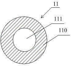
[0023] Embodiment 1, this embodiment proposes an anti-shedding pad, such as figure 1 As shown, it includes copper foil 11 mounted on the circuit board base material, the copper foil 11 is electrically connected with the circuit traces arranged on the circuit board base material, and the copper foil 11 includes a central solder resist located in the central area layer 110 and an oil-coated layer 111 located in the outer edge region, the upper surface of the oil-coated layer 111 is coated with a green oil layer. The anti-shedding pad of this embodiment divides the entire copper foil 11 into a central solder resist layer 110 located in the central area and an oil-coated layer 111 located in the outer edge area, and the upper surface of the oil-coated layer 111 is coated with a green oil layer (The reason for the angle is not shown in the figure). On the one hand, in order to meet the function of the pad, it is ensured that the exposed part of the copper foil (that is, the central...
Embodiment 2
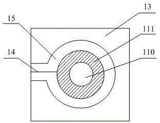
[0026] Embodiment 2, based on the anti-shedding pad in Embodiment 1, this embodiment proposes a circuit board, such as figure 2 As shown, it includes a circuit board base material 13, a circuit trace 14, and a pad electrically connected to the circuit trace 14, and the pad includes a copper foil 11 mounted on the circuit board base material, so The copper foil 11 includes a central solder resist layer 110 located in the central area and an oil-coated layer 111 located in the outer edge area, and the upper surface of the oil-coated layer 111 is coated with a green oil layer. like figure 2 As shown in , the pad is an independent copper foil 11 in the circuit board base material 13, and the surrounding area of the copper foil 11 is a clearance area 15, which is used to isolate the copper foil 11 from other copper areas on the circuit board, and the clearance The upper surface of the area 15 is also coated with a green oil layer. Therefore, it is preferable that the green oil...
Embodiment 3
[0030] Embodiment 3, based on a circuit board in Embodiment 2, this embodiment proposes a circuit board printing method. This circuit board printing method includes the step of attaching pads. The schematic structural diagram of the circuit board is as follows figure 2 As shown, the pad includes copper foil 11, and the step of attaching the pad includes:
[0031] S1. Mount the copper foil 11 on the circuit board substrate 13, and electrically connect the copper foil 11 to the circuit trace 14;
[0032] S2. The copper foil 11 includes a central solder resist layer 110 located in the central area and an oil-coated layer 111 located in the outer edge area, and the surface of the oil-coated layer 111 together with the clearance area 15 around the copper foil 11 is coated with green oil layer.
[0033]In this embodiment, by coating the surface of the oil-coated layer 111 together with the clear area 15 around the copper foil 11 with a green oil layer, the formed green oil layer h...
PUM
 Abstract
Description
Claims
Application Information
 - R&D Engineer
- R&D Manager
- IP Professional
- Industry Leading Data Capabilities
- Powerful AI technology
- Patent DNA Extraction
Browse by: Latest US Patents, China's latest patents, Technical Efficacy Thesaurus, Application Domain, Technology Topic, Popular Technical Reports.
© 2024 PatSnap. All rights reserved.Legal|Privacy policy|Modern Slavery Act Transparency Statement|Sitemap|About US| Contact US: help@patsnap.com