
Low-voltage and high-efficiency organic LED and preparation method thereof

A light-emitting diode, high-efficiency technology, applied in the direction of organic light-emitting devices, organic light-emitting device structures, organic semiconductor device materials, etc., can solve the problems of efficiency attenuation, narrow exciton formation area, etc., and achieve lower driving voltage, low driving voltage, The effect of delaying the decay of efficiency

Inactive Publication Date: 2015-03-11
TIANJIN UNIVERSITY OF TECHNOLOGY
View PDF6 Cites 14 Cited by
  • Summary
  • Abstract
  • Description
  • Claims
  • Application Information

AI Technical Summary

Problems solved by technology

The light-emitting layer of traditional OLED is a single-layer thin film, and the exciton formation area is relatively narrow, resulting in a rapid decline in OLED efficiency, and expanding the exciton formation area can solve the problem of efficiency attenuation

Method used


Image

  • Low-voltage and high-efficiency organic LED and preparation method thereof
  • Low-voltage and high-efficiency organic LED and preparation method thereof
  • Low-voltage and high-efficiency organic LED and preparation method thereof

Examples


Embodiment 1

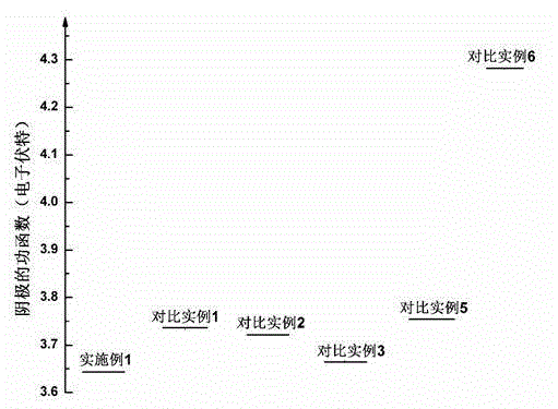
[0018] A low-voltage high-efficiency organic light-emitting diode, such as figure 1 As shown, it consists of a glass substrate with ITO, a hole transport layer, a p-type doped light-emitting layer, an i-type intrinsic light-emitting layer, an n-type doped light-emitting layer, an electron transport layer, a composite electron injection layer and a cathode A stacked structure is formed in sequence, in which the p-type doped light-emitting layer uses a hole transport material doped with a blue fluorescent dye; the i-type intrinsic light-emitting layer uses a blue fluorescent dye; the n-type doped light-emitting layer uses an electron doped with a blue fluorescent dye Transport material, the three-layer light-emitting layer is referred to as p-i-n light-emitting layer, the composite electron injection layer is composed of cesium carbonate inserted into a thin aluminum layer, and the thickness of each layer of film is 30nm for the hole transport layer, 12nm for the p-type doped lig...


PUM


Abstract

The invention provides a low-voltage and high-efficiency organic LED. The low-voltage and high-efficiency organic LED comprises a glass substrate with an ITO, a hole-transmission layer, a p type doped luminescence layer, an i type intrinsic luminescence layer, an n type doped luminescence layer, an electronic transmission layer, a composite electron injection layer and a cathode which are sequentially overlapped to form an overlapping layer; the p type doped luminescence layer is prepared through hole transmission material in which blue fluorescent dye is doped; the i type intrinsic luminescence is prepared through blue fluorescent dye; the n type doped luminescence layer is prepared through the electron transmission material in which blue fluorescent dye is doped; the three luminescence layers are named p-i-n type luminescence layer; and the composite electronic injection layer is prepared through cesium carbonate in which a thin aluminum layer is inserted. The low-voltage and high-efficiency organic LED has the advantages that the composite electron injection layer with a thin aluminum layer inserted into the cesium carbonate layer and the p-i-n type luminescence layer are arranged, so that the luminescence efficiency is improved, and the reduction of the efficiency is delayed; the driving voltage is low, the luminance is high, the efficiency is high, the stability is improved, and the preparation process is simple.

Description

technical field [0001] The invention belongs to the technical field of organic light-emitting diodes (OLEDs), and in particular relates to a low-voltage driving, high-efficiency organic light-emitting diode containing a composite electron injection layer and a p-i-n light-emitting layer and a preparation method thereof. Background technique [0002] With its outstanding advantages, organic light emitting diode (OLED) is gradually becoming a very popular emerging flat panel display product. It has the advantages of high brightness, wide viewing angle, low power consumption, fast response, simple preparation process and low cost. However, the hole transport ability of the organic semiconductor material is stronger than the electron transport ability, which will cause the number of holes in the light-emitting layer to be greater than the number of electrons, increase the driving voltage, and reduce the luminous efficiency of the organic light-emitting diode. Therefore, the mai...

Claims


Application Information

Patent Timeline
Patent Type & Authority Applications(China)
IPC IPC(8): H01L51/50H01L51/54H01L51/56
CPCH10K30/865H10K50/155H10K50/171H10K2102/00H10K2102/302H10K71/00
Inventor 吴晓明辛利文张欣于倩倩高建华玉林印寿根
Owner TIANJIN UNIVERSITY OF TECHNOLOGY
Learn More