
Method of manufacturing wiring board

A manufacturing method and wiring substrate technology, applied in the manufacture of printed circuits, removal of conductive materials by chemical/electrolytic methods, reinforcement of conductive patterns, etc., can solve problems such as the risk of damage to electrical insulation and complicated manufacturing processes, and achieve manufacturing Simple process and good electrical insulation effect

Inactive Publication Date: 2015-02-11
KYOCERA CORP
View PDF1 Cites 2 Cited by
  • Summary
  • Abstract
  • Description
  • Claims
  • Application Information

AI Technical Summary

Problems solved by technology

For this reason, when the distance between adjacent wiring conductors 12 is as narrow as, for example, 20 μm or less, there is a risk that the electrical insulation between adjacent wiring conductors 12 will be impaired due to solder that spreads to the side surfaces of wiring conductors 12. high sex
In addition, it is necessary to etch the base metal layer 12a at the portion not covered with the main conductor layer 12b twice, and the manufacturing process is complicated.

Method used


Image

  • Method of manufacturing wiring board
  • Method of manufacturing wiring board
  • Method of manufacturing wiring board

Examples


Embodiment Construction

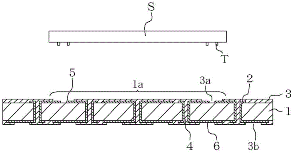
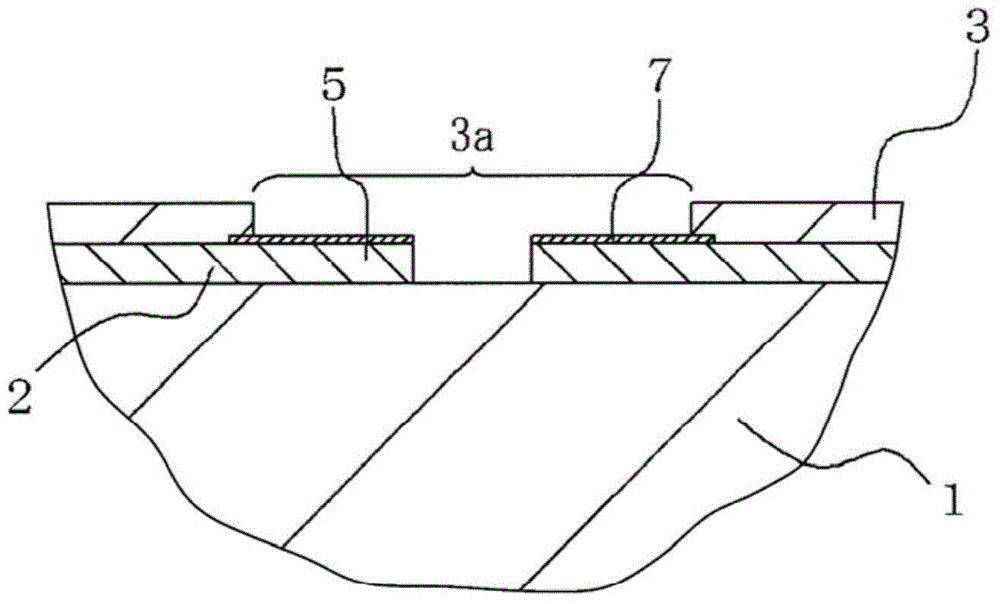
[0054] Next, the method of manufacturing the wiring board of the present invention will be explained based on the drawings. figure 1 It is a schematic cross-sectional view showing an example of a wiring board manufactured by the method of the present invention. figure 2 Yes figure 1 A schematic top view of the wiring board shown. image 3 Yes figure 1 An enlarged cross-sectional view of the main part of the wiring board shown.

[0055] The wiring board includes an insulating substrate 1, a wiring conductor 2, and a solder resist layer 3. in figure 2 In the figure, a dotted line indicates the portion covered by the solder resist layer 3 in the wiring conductor 2 on the upper surface of the insulating substrate 1.

[0056] The insulating substrate 1 is made of a resin-based electrical insulating material that heats a single-layer or multiple-layer insulating layer. The insulating layer is obtained by impregnating a glass cloth base material with a thermosetting resin such as epo...


PUM

PropertyMeasurementUnit
diameteraaaaaaaaaa
thicknessaaaaaaaaaa
thicknessaaaaaaaaaa

Abstract

A manufacturing method includes a step of forming a first plating mask on a base metal layer, a step of forming a main conductor layer on the base metal layer exposed from the first plating mask, a step of forming a second plating mask on them, a step of attaching a metal plating layer to an upper surface of the main conductor layer exposed from the second plating mask, a step of removing the first and second plating masks, a step of etching away a portion of the base metal layer to which the main conductor layer is not attached, and a step of forming a solder resist layer.

Description

Technical field [0001] The present invention relates to a method of manufacturing a wiring board for mounting semiconductor elements such as semiconductor integrated circuit elements. Background technique [0002] The wiring board for mounting the semiconductor element has a wiring conductor made of copper for electrical connection with the semiconductor element on the upper surface of the insulating substrate. Furthermore, the upper surface of the insulating substrate is covered with a solder resist layer so that a part of the wiring conductor electrically connected to the semiconductor element is exposed. In addition, the surface of the wiring conductor exposed from the solder resist layer is covered with a plated metal layer with excellent solder wettability. Then, the electrode of the semiconductor element is connected to the wiring conductor covered with the plated metal layer via solder. As a plating metal layer with excellent solder wettability, a gold plating layer base...

Claims


Application Information

Patent Timeline
Patent Type & Authority Applications(China)
IPC IPC(8): H05K3/24H05K3/18
CPCH05K2203/0548H05K3/07H05K2203/0582H05K3/061H05K2203/0369H05K3/108H05K3/243H05K3/244H05K3/3436H05K2201/09409H05K2203/0574H05K2203/0597
Inventor 大隅孝一野口澄子
Owner KYOCERA CORP
Learn More