Voltage level switching circuit

A technology for converting circuits and voltage levels, which is applied in the direction of logic circuit connection/interface layout, etc., can solve the problems of difficult transition, circuit leakage, and increased power consumption, so as to shorten the rise and fall time, reduce the circuit area, and save costs. Effect

Inactive Publication Date: 2015-02-11
ILI TECHNOLOGY CORPORATION
View PDF5 Cites 2 Cited by
  • Summary
  • Abstract
  • Description
  • Claims
  • Application Information

AI Technical Summary

Problems solved by technology

[0010] However, when the voltage levels of the input signal IN and the inverted input signal INB are close to the threshold voltages of the input stage transistors (namely, the first transistor M1 and the second transistor M2), they will encounter difficulty in transition, which will easily cause There is a direct current (DC) current in the circuit when it is static, resulting in leakage current in the circuit
[0011] Generally, in order to overcome this problem, the dynamic current of the input stage transistor will be increased by increasing the width of the input stage transistor, or the channel length (channel length) of the transistor of the latch circuit (that is, the third transistor M3 and the fourth transistor M4) will be increased. ) to reduce the ability of the latch circuit, but the former not only increases the power consumption but also increases the layout area and increases the circuit cost. The latter is an N type Metal-Oxide-Semiconductor field-effect transistor for the input stage transistor. Field-Effect Transistor, abbreviated as N-MOSFET), will increase the rise time (rising time) of the output signal OUT and the inverted output signal OUTB. For the input stage transistor, it is a P-type metal oxide semi-field effect transistor (P-MOSFET ) (such as figure 2 shown), it will increase the falling time (falling time) of the output signal OUT and the inverted output signal OUTB, resulting in an increase in the transition time

Method used


Image

  • Voltage level switching circuit
  • Voltage level switching circuit
  • Voltage level switching circuit

Examples


Embodiment Construction

[0045] Below in conjunction with accompanying drawing and embodiment the present invention is described in detail:

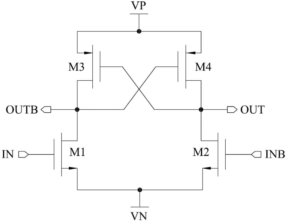
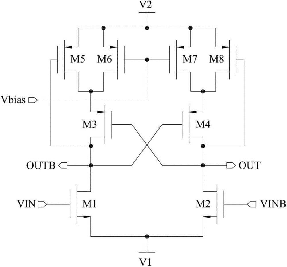
[0046] refer to image 3 , The first preferred embodiment of the voltage level conversion circuit of the present invention includes a first output terminal OUT and a second output terminal OUTB, a first transistor M1, a second transistor M2, a third transistor M3, a first Four transistors M4, a fifth transistor M5, a sixth transistor M6, a seventh transistor M7, an eighth transistor M8, and a bias input terminal Vbias.

[0047] The first output terminal OUT and the second output terminal OUTB are respectively used to output a first output voltage and a second output voltage complementary to the first output voltage.

[0048] The first transistor M1 includes a first terminal electrically connected to the second output terminal OUTB, a second terminal electrically connected to a first level voltage V1, and a control terminal receiving a first input voltage VIN. ...


PUM


Abstract

The invention provides a voltage level switching circuit. The voltage level switching circuit comprises a first transistor, a second transistor, a third transistor, a fourth transistor, a fifth transistor, a sixth transistor, a seventh transistor and an eighth transistor. The sixth transistor and the seventh transistor are arranged to provide equivalent high resistance, and the latch capacity of the third transistor and the fourth transistor is reduced. When the voltage difference of the input voltage is in a low level, the state of the circuit can be switched smoothly. The fifth transistor and the eighth transistor are arranged to provide a breakover path, the rising time or the falling time of output signals can be shortened. Under the demand of the same switching time, compared with the prior art, the voltage level switching circuit is advantaged in that the layout area and dynamic current consumption can be reduced.

Description

technical field [0001] The invention relates to a conversion circuit, in particular to a voltage level conversion circuit. Background technique [0002] A voltage level conversion circuit is a conversion circuit widely used in current electronic circuits, and is used for converting signals between different voltage levels. [0003] refer to figure 1 , there is a voltage level conversion circuit ( figure 1 Using an N-Type voltage level conversion circuit for illustration) includes a first transistor M1 , a second transistor M2 , a third transistor M3 , and a fourth transistor M4 . [0004] The first transistor M1 has a first terminal outputting an inverted output signal OUTB, a second terminal electrically connected to a low level voltage VN, and a control terminal receiving an input signal IN. [0005] The second transistor M2 has a first terminal outputting an output signal OUT, a second terminal electrically connected to the low level voltage VN, and a control terminal ...

Claims


Application Information

Patent Timeline
Patent Type & Authority Applications(China)
IPC IPC(8): H03K19/0175
Inventor 杨家睿叶松铫
Owner ILI TECHNOLOGY CORPORATION
Why Eureka
Try Eureka