
Resistive memory and manufacturing method thereof

A resistive memory, electrode technology, applied in static memory, digital memory information, information storage, etc., can solve the problems of poor reset efficiency, increase the time of applying negative bias, and achieve the effect of improving reset efficiency

Inactive Publication Date: 2015-02-11
WINBOND ELECTRONICS CORP
View PDF10 Cites 3 Cited by
  • Summary
  • Abstract
  • Description
  • Claims
  • Application Information

AI Technical Summary

Problems solved by technology

Therefore, it is often necessary to apply a higher negative bias voltage and increase the time to apply the negative bias voltage, resulting in poor reset efficiency

Method used


Image

  • Resistive memory and manufacturing method thereof
  • Resistive memory and manufacturing method thereof
  • Resistive memory and manufacturing method thereof

Examples


Embodiment Construction

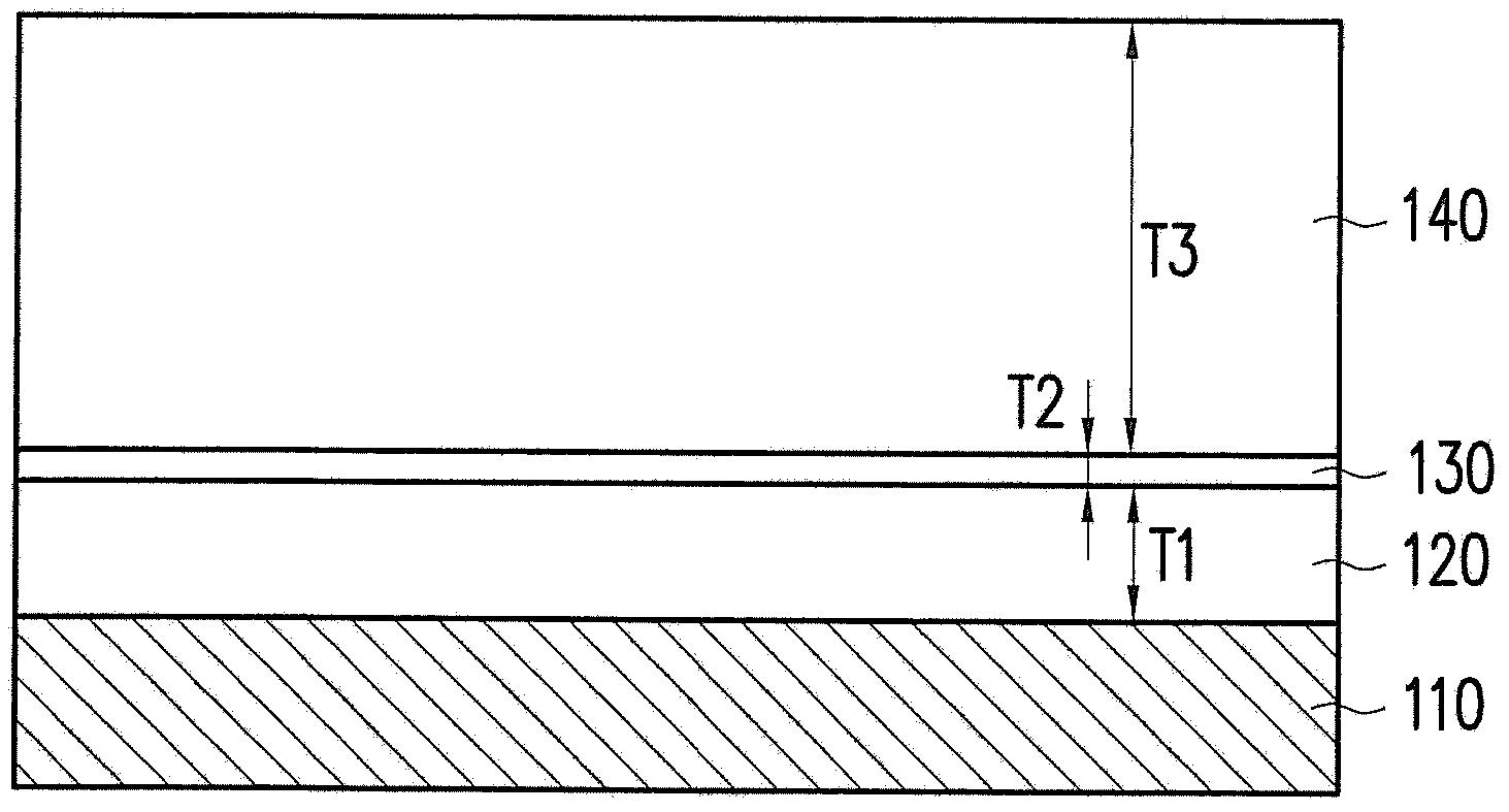
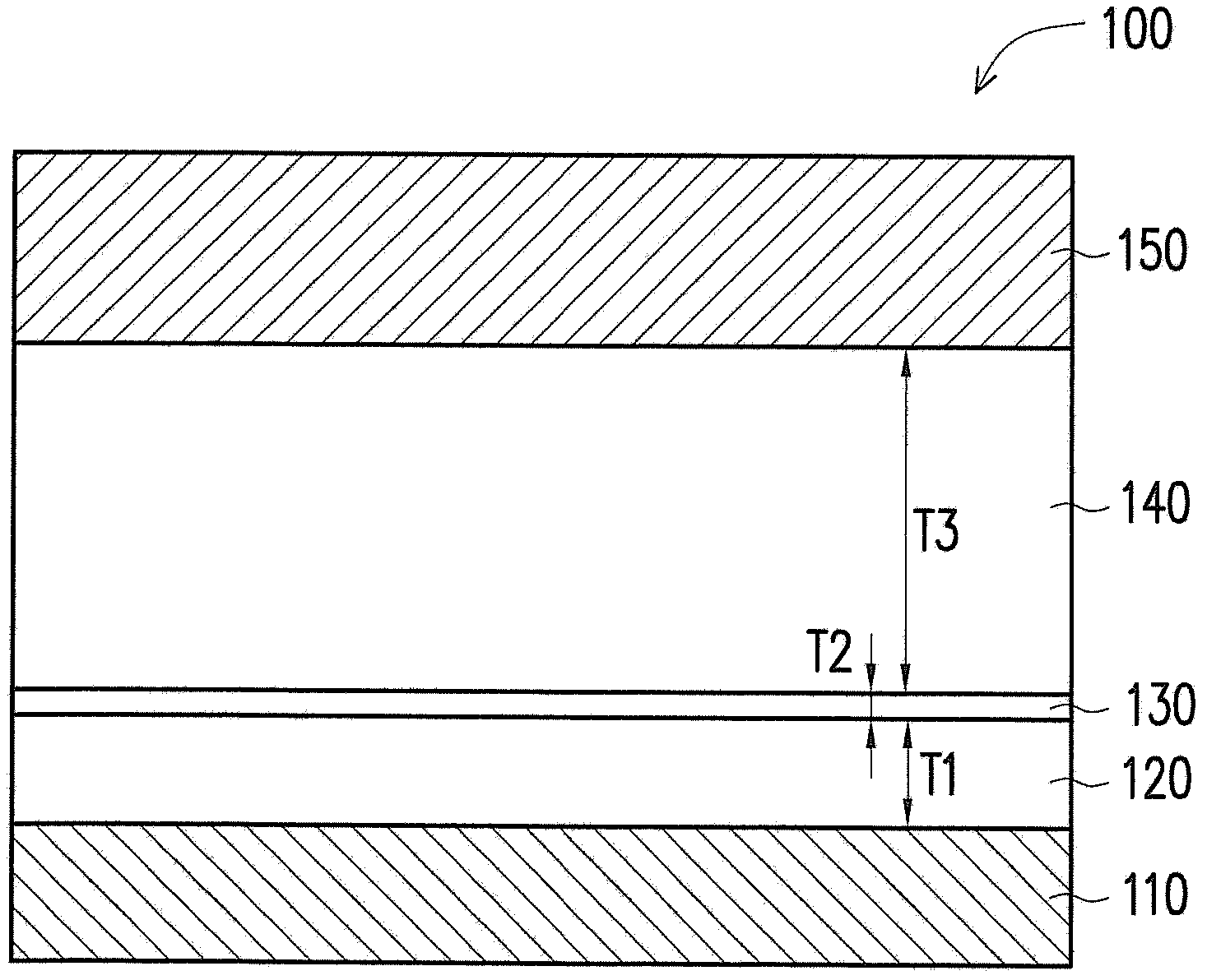
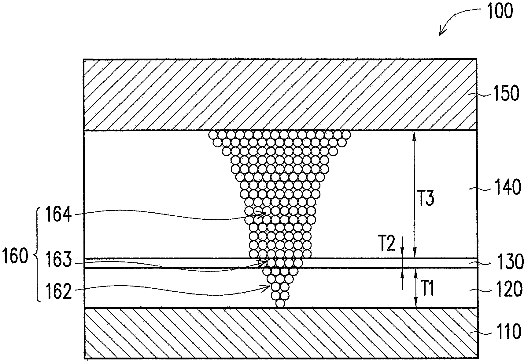
[0027] Figure 1A to Figure 1B It is a schematic cross-sectional view of a manufacturing method of the resistive memory 100 according to an embodiment of the present invention. First, please refer to Figure 1A , forming a first dielectric layer 120 on the first electrode 110 . The material of the first electrode 110 is, for example, titanium nitride (TiN), platinum (Pt), iridium (Ir), ruthenium (Ru), titanium (Ti), tungsten (W), tantalum (Ta), aluminum (Al), Zirconium (Zr), hafnium (Hf), nickel (Ni), copper (Cu), cobalt (Co), iron (Fe), gadolinium (Y) or manganese (Mo) can be formed by physical vapor deposition, for example. The material of the first dielectric layer 120 is, for example, hafnium oxide (such as HfO or HfO 2 etc.), lanthanum oxide, gadolinium oxide, yttrium oxide, zirconium oxide, titanium oxide, tantalum oxide, nickel oxide, tungsten oxide, copper oxide, cobalt oxide or iron oxide, formed by chemical vapor deposition, for example.

[0028] please refer agai...


PUM

PropertyMeasurementUnit
thicknessaaaaaaaaaa
thicknessaaaaaaaaaa

Abstract

The invention discloses a resistive memory and a manufacturing method thereof. The resistive memory comprises a first electrode, a second electrode, a first dielectric layer, a second dielectric layer and a third dielectric layer, wherein the first electrode is opposite to the second electrode. In a process of setting the resistive memory, currents flow from the second electrode to the first electrode; in a process of resetting the resistive memory, the currents flow from the first electrode to the second electrode; the first dielectric layer is arranged between the first electrode and the second electrode; the second dielectric layer is arranged between the first dielectric layer and the second electrode layer; the third dielectric layer is arranged between the second dielectric layer and the second electrode; the first dielectric layer and the third dielectric layer are made of the same material; the material of the second dielectric layer is different from that of the first dielectric layer and the third dielectric layer.

Description

technical field [0001] The present invention relates to a memory and its manufacturing method, and in particular to a resistive memory and its manufacturing method. Background technique [0002] In recent years, the development of resistive memory (such as resistive random access memory (Resistive Random Access Memory, RRAM) is extremely fast, and it is currently the most attention-grabbing structure of future memory. Because resistive memory has low power consumption, high-speed operation, high Density and compatibility with complementary metal oxide semiconductor (Complementary Metal Oxide Semiconductor, CMOS) process technology potential advantages, so it is very suitable as the next generation of non-volatile memory devices. [0003] The current resistive memory generally includes an upper electrode and a lower electrode disposed opposite to each other and a dielectric layer between the upper electrode and the lower electrode. When setting the current resistive memory, ...

Claims


Application Information

Patent Timeline
Patent Type & Authority Applications(China)
IPC IPC(8): H01L45/00G11C13/00
Inventor 许博砚沈鼎瀛江明崇魏敏芝
Owner WINBOND ELECTRONICS CORP
Learn More