Injection Enhanced Insulated Gate Bipolar Transistor
A bipolar transistor, injection enhancement technology, applied in semiconductor devices, electrical components, circuits, etc., can solve the problem of low carrier concentration, increase carrier concentration, increase process difficulty, and reduce conduction voltage drop Effect
- Summary
- Abstract
- Description
- Claims
- Application Information
AI Technical Summary
Problems solved by technology
Method used
Image
Examples
Embodiment 1
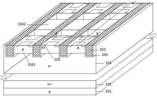
[0042] The injection-enhanced insulated gate bipolar transistor includes a p-type collector 101, and a carrier diffusion layer 103 is arranged on the p-type collector 101, and a plurality of grooves are vertically arranged on the carrier diffusion layer 103 202, multiple rows of p-type active regions 1041 and p-type inactive regions 1042 are arranged laterally on the carrier diffusion layer 103, and the p-type active regions 1041 and p-type inactive regions 1042 form a p-type base region in a stripe shape Each row of p-type active regions 1041 includes a plurality of independent p-type active regions 1041, which are separated by the trench 202 between the plurality of p-type active regions 1041, and each row of p-type inactive regions 1042 includes a plurality of independent A p-type inactive region 1042, a plurality of p-type inactive regions 1042 are separated by the trench 202; each p-type active region 1041 is provided with an n-type emitter 105, and the n-type emitter 105...
Embodiment 2
[0045] The injection-enhanced insulated gate bipolar transistor includes a p-type collector 101, and a carrier diffusion layer 103 is arranged on the p-type collector 101, and a plurality of grooves are vertically arranged on the carrier diffusion layer 103 202, multiple rows of p-type active regions 1041 and p-type inactive regions 1042 are arranged laterally on the carrier diffusion layer 103, and the p-type active regions 1041 and p-type inactive regions 1042 form a p-type base region in a stripe shape Each row of p-type active regions 1041 includes a plurality of independent p-type active regions 1041, which are separated by the trench 202 between the plurality of p-type active regions 1041, and each row of p-type inactive regions 1042 includes a plurality of independent A p-type inactive region 1042, a plurality of p-type inactive regions 1042 are separated by the trench 202; each p-type active region 1041 is provided with an n-type emitter 105, and the n-type emitter 105...
Embodiment 3
[0051] The injection-enhanced insulated gate bipolar transistor includes a p-type collector 101, and a carrier diffusion layer 103 is arranged on the p-type collector 101, and a plurality of grooves are vertically arranged on the carrier diffusion layer 103 202, multiple rows of p-type active regions 1041 and p-type inactive regions 1042 are arranged laterally on the carrier diffusion layer 103, and the p-type active regions 1041 and p-type inactive regions 1042 form a p-type base region in a stripe shape Each row of p-type active regions 1041 includes a plurality of independent p-type active regions 1041, which are separated by the trench 202 between the plurality of p-type active regions 1041, and each row of p-type inactive regions 1042 includes a plurality of independent A p-type inactive region 1042, a plurality of p-type inactive regions 1042 are separated by the trench 202; each p-type active region 1041 is provided with an n-type emitter 105, and the n-type emitter 105...
PUM
 Abstract
Description
Claims
Application Information
 - R&D
- Intellectual Property
- Life Sciences
- Materials
- Tech Scout
- Unparalleled Data Quality
- Higher Quality Content
- 60% Fewer Hallucinations
Browse by: Latest US Patents, China's latest patents, Technical Efficacy Thesaurus, Application Domain, Technology Topic, Popular Technical Reports.
© 2025 PatSnap. All rights reserved.Legal|Privacy policy|Modern Slavery Act Transparency Statement|Sitemap|About US| Contact US: help@patsnap.com


