
A method of manufacturing silicon epitaxial wafers for fast recovery diodes

A silicon epitaxial wafer, rapid recovery technology, applied in semiconductor/solid-state device manufacturing, electrical components, circuits, etc., can solve the problems of difficult uniformity of resistivity and difficulty in epitaxial layer process, etc. character defects, promote the effect of improvement

Active Publication Date: 2017-07-07
CHINA ELECTRONICS TECH GRP NO 46 RES INST +1
View PDF6 Cites 0 Cited by
  • Summary
  • Abstract
  • Description
  • Claims
  • Application Information

AI Technical Summary

Problems solved by technology

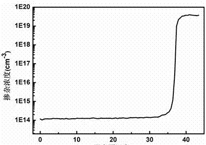
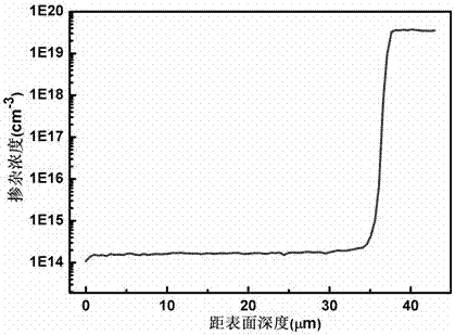
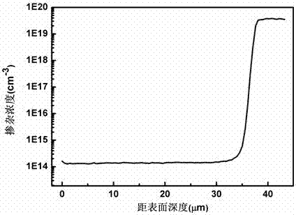
Silicon epitaxial wafers for fast recovery diodes need to grow high-resistance epitaxial layers on heavily doped silicon substrates. Affected by the self-doping effect of substrate impurity volatilization, it is difficult to prepare epitaxial layers with high resistivity uniformity and narrow transition regions. , especially when the required epitaxial layer thickness is thicker and the growth time is longer, it is more difficult to obtain an epitaxial layer with high resistivity uniformity and narrow transition region width

Method used


Image

  • A method of manufacturing silicon epitaxial wafers for fast recovery diodes
  • A method of manufacturing silicon epitaxial wafers for fast recovery diodes
  • A method of manufacturing silicon epitaxial wafers for fast recovery diodes

Examples


Embodiment 1

[0023] (1) First use HCl to etch the base of the epitaxial furnace at high temperature to remove the residual deposits on the base. The temperature is set at 1120°C, the flow rate of HCl gas is set at 3 L / min, and the etching time is set at It was set at 5 min, and then the base was re-wrapped with a layer of intrinsic polysilicon, the growth material was trichlorosilane gas, the flow rate was set at 35 g / min, and the time was set at 10 min.

[0024] (2) A silicon substrate is placed in the pit of the base of the epitaxial furnace. The conductivity type of the silicon wafer is N-type, the crystal orientation is , the resistivity is 0.002 Ωcm, the thickness is 525 μm, and the diameter is 125 mm. The reaction chamber of the epitaxial furnace was purged with nitrogen and hydrogen in sequence for 10 minutes, and the gas flow rate was set at 100 L / min.

[0025] (3) Carry out vapor phase polishing on the surface of the silicon substrate, set the temperature at 1150 °C, use hydrogen ...

Embodiment 2

[0034] (1) First use HCl to etch the base of the epitaxial furnace at high temperature to remove the residual deposits on the base. The temperature is set at 1120°C, the flow rate of HCl gas is set at 2 L / min, and the etching time is set at It was set at 4 minutes, and then the base was re-coated with a layer of intrinsic polysilicon. The growth material was trichlorosilane gas, the flow rate was set at 35 g / min, and the time was set at 10 minutes.

[0035](2) A silicon substrate is placed in the pit of the base of the epitaxial furnace. The conductivity type of the silicon wafer is N-type, the crystal orientation is , the resistivity is 0.002 Ωcm, the thickness is 525 μm, and the diameter is 125 mm. The reaction chamber of the epitaxial furnace was purged with nitrogen and hydrogen in sequence for 8 minutes, and the flow rate was set at 120 L / min.

[0036] (3) Perform vapor phase polishing on the surface of the silicon substrate, set the temperature at 1180 °C, use hydrogen t...

Embodiment 3

[0045] (1) First use HCl to etch the base of the epitaxial furnace at high temperature to remove the residual deposits on the base. The temperature is set at 1120°C, the flow rate of HCl gas is set at 3 L / min, and the etching time is set at It was set at 5 min, and then the base was re-wrapped with a layer of intrinsic polysilicon, the growth material was trichlorosilane gas, the flow rate was set at 35 g / min, and the time was set at 10 min.

[0046] (2) A silicon substrate is placed in the pit of the base of the epitaxial furnace. The conductivity type of the silicon wafer is N-type, the crystal orientation is , the resistivity is 0.002 Ωcm, the thickness is 525 μm, and the diameter is 125 mm. The reaction chamber of the epitaxial furnace was purged with nitrogen and hydrogen in sequence for 8 minutes, the purity of nitrogen and hydrogen were both ≥99.999%, and the flow rate was set at 100 L / min.

[0047] (3) Perform vapor phase polishing on the surface of the silicon substra...


PUM

PropertyMeasurementUnit
thicknessaaaaaaaaaa
diameteraaaaaaaaaa
widthaaaaaaaaaa

Abstract

The invention relates to a manufacture method of a silicon epitaxial slice for a fast recovery diode. The manufacture method of the silicon epitaxial slice for the fast recovery diode improves the thickness of an epitaxial slice and uniformity of electrical resistivity parameters and reduces occurrence rate of crystal defects by optimizing an existing technology and restraining self doping effects, and thereby meets use requirements of fast recovery diode devices, and greatly improves reliability and finished product rate of the fast recovery diode devices. Thickness non-uniformity of the silicon epitaxial slice prepared through the manufacture method of the silicon epitaxial slice for the fast recovery diode is less than 1%. Electrical resistivity non-uniformity of the silicon epitaxial slice is less than 2%. No lattice defect exists in the silicon epitaxial slice. The thickness of a transition area is less than 4 micrometers. Parameters of the silicon epitaxial slice prepared through the manufacture method of the silicon epitaxial slice for the fast recovery diode fully meets requirements of the fast recovery diode devices for silicon epitaxial materials. The silicon epitaxial slice prepared through the manufacture method of the silicon epitaxial slice for the fast recovery diode obtains general consent of users at present, and greatly propels improvement of performance of the domestic fast recovery diode devices.

Description

technical field [0001] The invention relates to the preparation technology of semiconductor materials, in particular to a method for manufacturing silicon epitaxial wafers for fast recovery diodes. Background technique [0002] The fast recovery diode has the ability of fast turn-on and high-speed turn-off, and its reverse recovery time is short, the forward voltage drop is low, and the reverse breakdown voltage is high. Fast recovery diodes are mainly used in high-frequency and high-power electronic circuits such as pulse width modulators, frequency converters, ultrasonic power supplies, and switching power supplies. Silicon epitaxial wafers are the key basic materials for preparing fast recovery diode devices. There are three important parameters to measure their performance, namely thickness, resistivity and surface defects. At present, it is generally required that the thickness non-uniformity of the epitaxial layer is ≤3%, the resistivity non-uniformity is ≤5%, and the...

Claims


Application Information

Patent Timeline
Patent Type & Authority Patents(China)
IPC IPC(8): H01L21/205H01L21/329
CPCH01L21/02381H01L21/02532H01L29/6609
Inventor 王文林李扬高航李明达
Owner CHINA ELECTRONICS TECH GRP NO 46 RES INST
Learn More