


Quick Research
Generate reliable direction feasibility study reports for your R&D in just a few steps.

Technical Q&A
Discover and master advanced knowledge NOW. Basics, ideas, possibilities, all at once.

Find Solutions
As an expert in R&D theories, this can generate solutions to your technical problems instantly.

Evaluate Feasibility
Analyze your overall solution with one click, know your potential R&D risks in advance.

Monitor Landscape
Get weekly tech updates, stay abreast of the latest tech innovations and key insights.
Electrostatic discharge structure and chip with the same
An electrostatic discharge and chip technology, applied in the field of electrostatic discharge structures, can solve problems such as increasing the burden on integrated circuits and reducing system performance, and achieve the effect of improving robustness
- Summary
- Abstract
- Description
- Claims
- Application Information
AI Technical Summary
Problems solved by technology
Method used
Image

Examples
Embodiment Construction
[0018] The following description is a preferred mode for carrying out the present invention. However, this preferred embodiment is only used to explain the present invention, not to limit the present invention. Therefore, the protection scope of the present invention should be determined by the scope described in the claims.
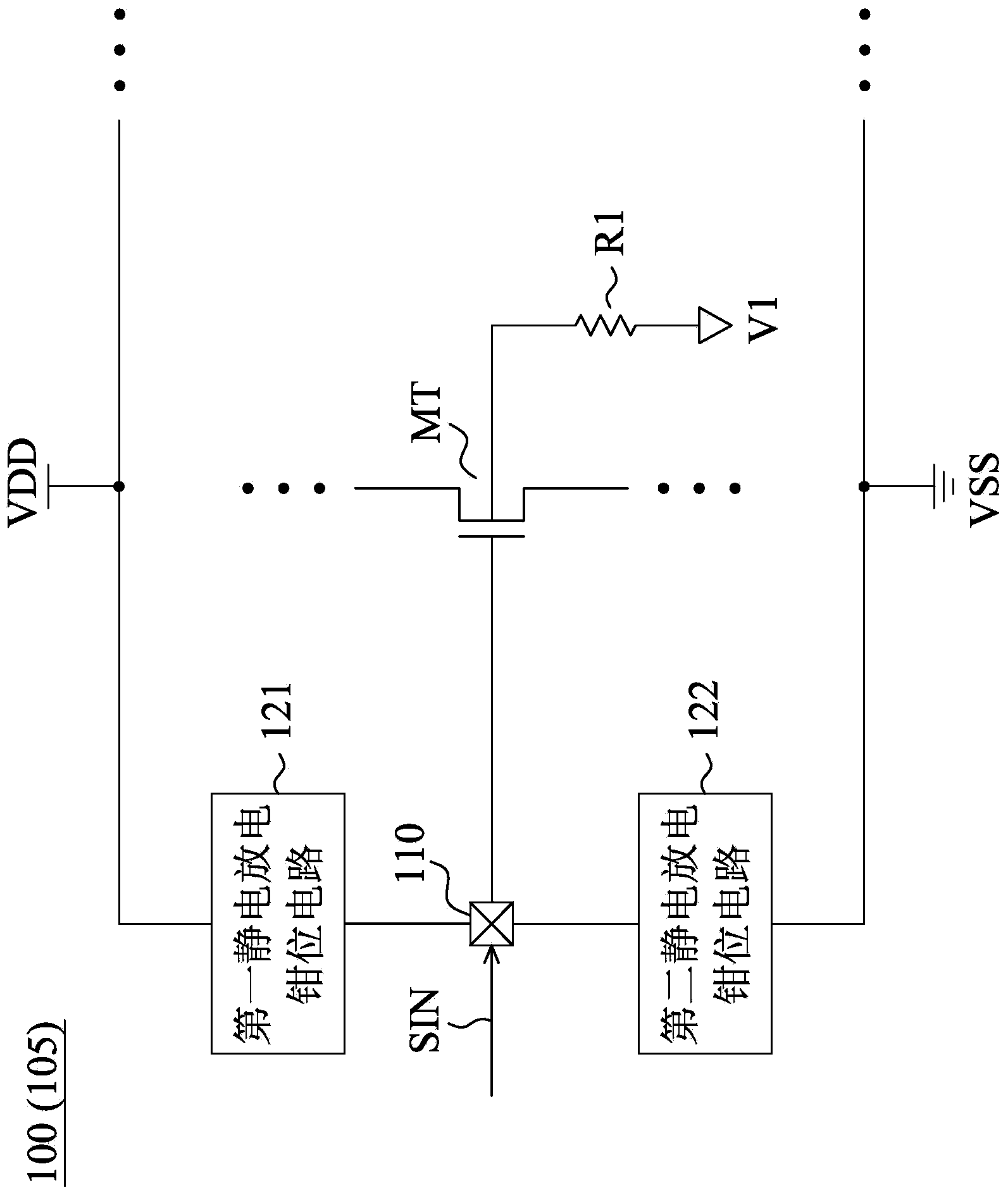
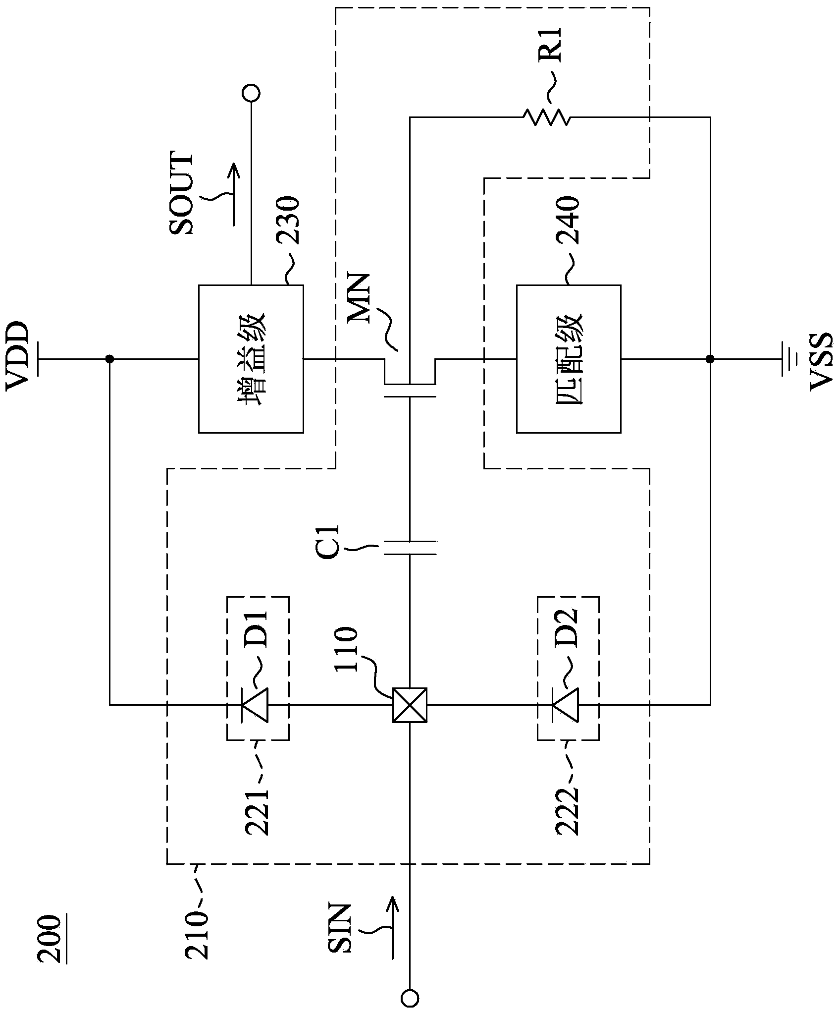
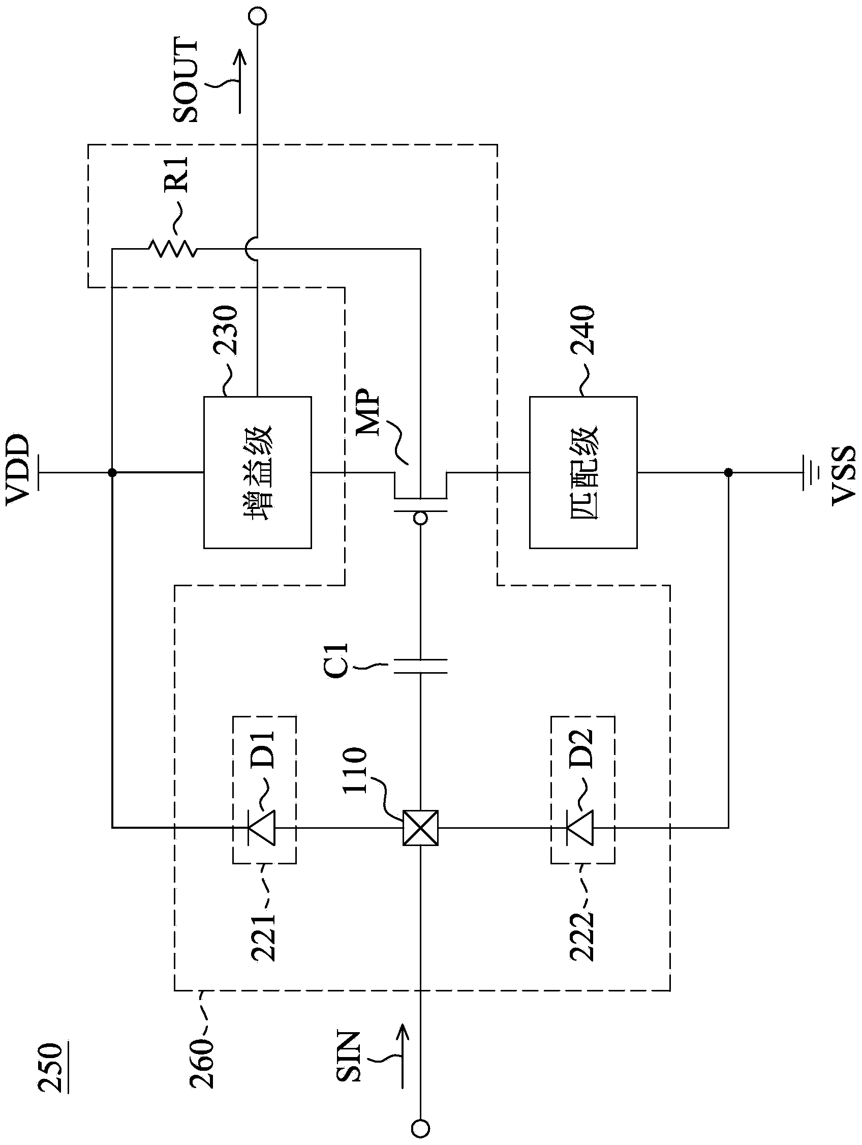
[0019] figure 1 It is a schematic diagram of an electrostatic discharge (Electrostatic discharge, ESD) structure 100 for improving the robustness of a charging device model (Charge Device Model, CDM) according to an embodiment of the present invention. The ESD structure 100 includes at least an input stage 105 . Such as figure 1 As shown, the input stage 105 includes an input pad 110 , a first ESD clamping circuit 121 , a second ESD clamping circuit 122 , a resistor R1 and a transistor MT. The input stage 105 can be coupled to other circuits (eg, the input terminal of an amplifier, but not limited thereto).
[0020] The input pad 110 is configured t...
PUM
 Abstract
Description
Claims
Application Information
 - R&D Engineer
- R&D Manager
- IP Professional
- Industry Leading Data Capabilities
- Powerful AI technology
- Patent DNA Extraction
Browse by: Latest US Patents, China's latest patents, Technical Efficacy Thesaurus, Application Domain, Technology Topic, Popular Technical Reports.
© 2024 PatSnap. All rights reserved.Legal|Privacy policy|Modern Slavery Act Transparency Statement|Sitemap|About US| Contact US: help@patsnap.com