Touch control type flat panel display
A flat-panel display and flat-panel display technology, which is applied to static indicators, instruments, and electrical digital data processing, etc., can solve the problems of increasing the number of lead-out electrode lines, deteriorating display light transmittance, and loss of display effect, so as to prevent signal loss. The effect of crosstalk
- Summary
- Abstract
- Description
- Claims
- Application Information
AI Technical Summary
Problems solved by technology
Method used
Image
Examples
specific Embodiment approach 1
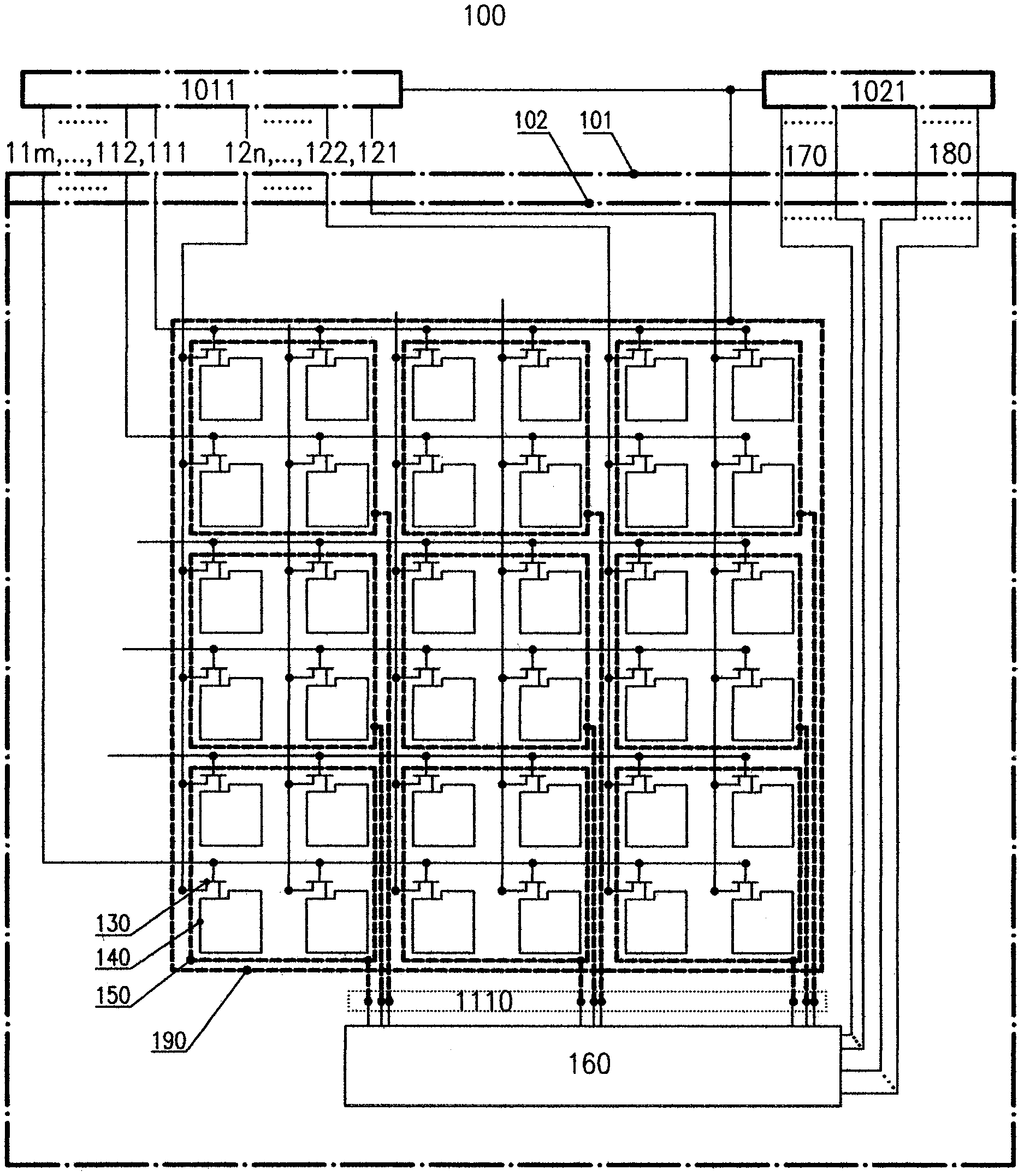
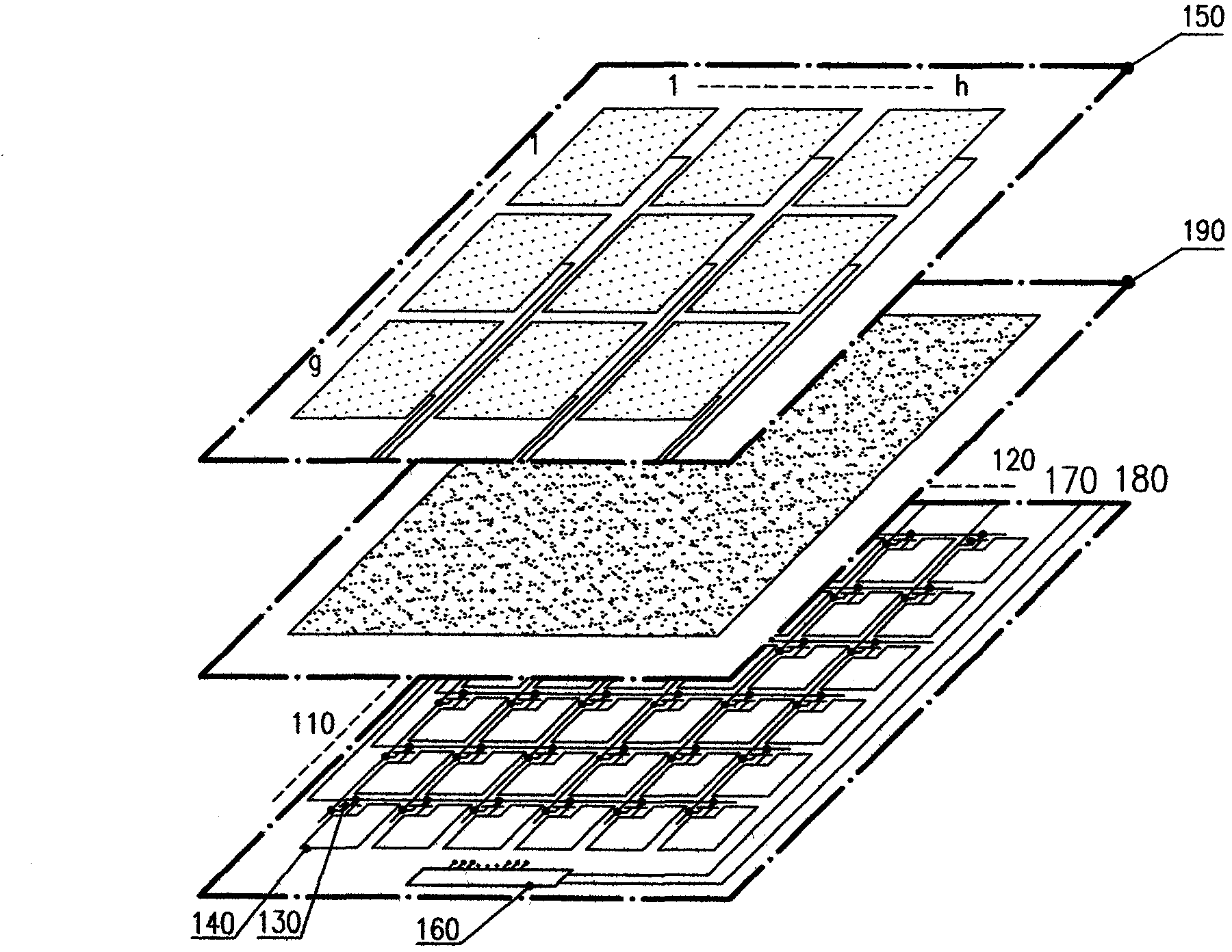
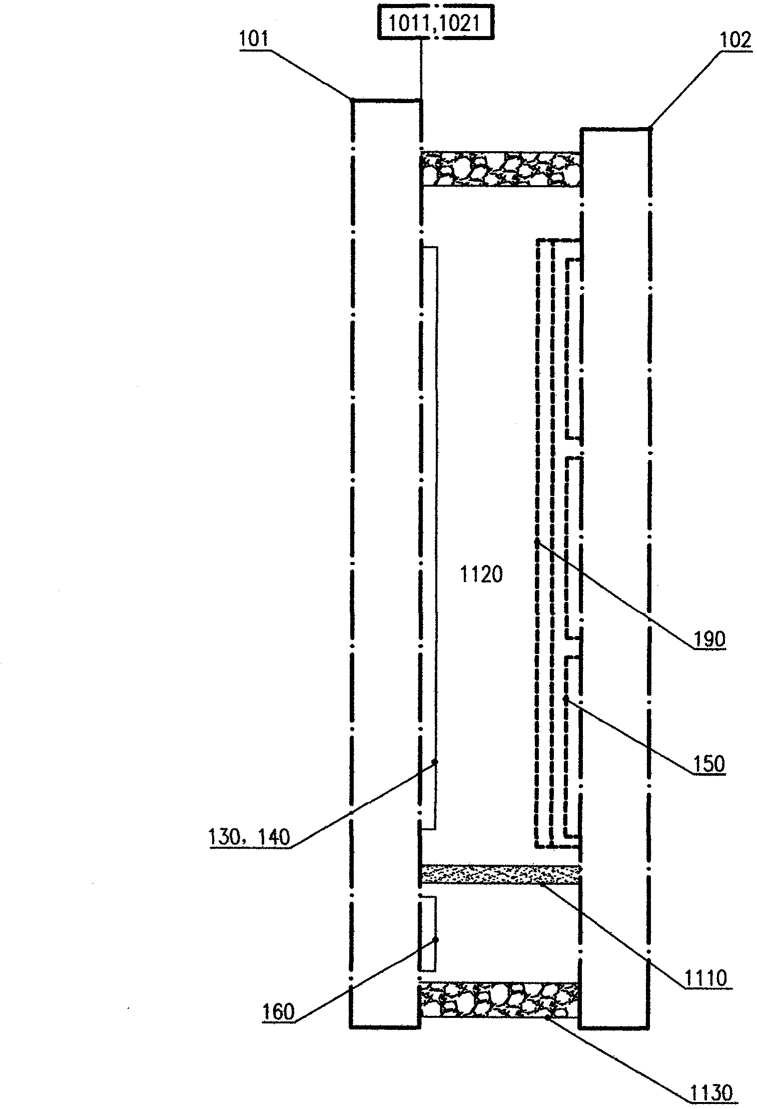
[0037] Such as figure 1 In the touch panel display 100 shown, the schematic diagram of the electrode structure of each layer is as follows: Figure 1a As shown, its side view is shown as Figure 1b As shown, the touch panel display 100 includes an active display panel and touch sensing electrodes. The display panel has a lower substrate 101 and an upper substrate 102. The two substrates are pasted together by an adhesive 1130. The area surrounded by the two substrates is Filled with LCD 1120. The inner surface of the upper substrate 102 has display common electrodes 190; the inner surface of the lower substrate 101 has display row scan electrode line groups 110, display column signal electrode line groups 120, (m×n) display active devices (such as thin films) Field Effect Transistor (TFT) unit array 130 and (m×n) display pixel electrode unit array 140, display row scanning electrode line group 110 includes 111, 112, ..., 11m scanning electrode lines, display column signal el...
specific Embodiment approach 2
[0045] Such as figure 2 The shown touch panel display 200 includes an active display panel and touch sensing electrodes, and the display panel has a lower substrate 201 and an upper substrate 202 . The inner surface of the lower substrate 201 has a display row scan electrode line group 210, a display column signal electrode line group 220, a (m×n) display thin film field effect transistor (TFT) unit array 230 and (m×n) display pixels The electrode unit array 240 shows that the row scanning electrode line group 210 includes 211, 212, ..., 21m scanning electrode lines, and the column signal electrode line group 220 includes 221, 222, ..., 22n signal electrode lines, where m and n are greater than A natural number of 2; the drains (Drain) of each TFT unit of the display TFT array 230 are connected to each unit of the display pixel electrode unit array 240 respectively, and the grid (Gate) is respectively connected to each electrode line of the display row scanning electrode line...
specific Embodiment approach 3
[0052] Such as image 3 The shown touch panel display 300 includes an active display panel and touch sensing electrodes, and the display panel has a lower substrate 301 and an upper substrate 302 . The inner surface of the upper substrate 302 has a display common electrode 390; the inner surface of the lower substrate 301 has a display row scan electrode line group 310, a display column signal electrode line group 320, and (m×n) display thin film field effect transistors (TFTs). ) unit array 330 and (m×n) display pixel electrode unit array 340, the display row scanning electrode line group 310 includes 311, 312, ..., 31m scanning electrode lines, and the display column signal electrode line group 320 includes 321, 322, ..., 32n signal electrode lines, m and n are natural numbers greater than 2; the drains (Drain) of each TFT unit of the display TFT array 330 are connected to the units of the display pixel electrode unit array 340, and the gates (Gate) are respectively connecte...
PUM
 Abstract
Description
Claims
Application Information
 - R&D
- Intellectual Property
- Life Sciences
- Materials
- Tech Scout
- Unparalleled Data Quality
- Higher Quality Content
- 60% Fewer Hallucinations
Browse by: Latest US Patents, China's latest patents, Technical Efficacy Thesaurus, Application Domain, Technology Topic, Popular Technical Reports.
© 2025 PatSnap. All rights reserved.Legal|Privacy policy|Modern Slavery Act Transparency Statement|Sitemap|About US| Contact US: help@patsnap.com


