Display device and manufacturing method thereof

A technology for a display device and a manufacturing method, which is applied in lamination devices, lighting devices, chemical instruments and methods, etc., can solve the problems of OCA optical adhesive layer thickness, device overall structure thickening, ink gap, etc., and achieve a thinner overall structure , reduce the thickness, reduce the effect of the gap

Inactive Publication Date: 2014-12-17
EVERDISPLAY OPTRONICS (SHANGHAI) CO LTD
View PDF6 Cites 6 Cited by
  • Summary
  • Abstract
  • Description
  • Claims
  • Application Information

AI Technical Summary

Problems solved by technology

[0004] The purpose of the present invention is to overcome the defects of the prior art, and provide a display device and its manufacturing method, which can solve the problem that the existence of ink gaps makes the OCA optical adhesive layer thicker and the overall structure of the device becomes thicker.

Method used


Image

  • Display device and manufacturing method thereof
  • Display device and manufacturing method thereof
  • Display device and manufacturing method thereof

Examples


Embodiment Construction

[0029] The present invention will be further described below in conjunction with the accompanying drawings and specific embodiments.

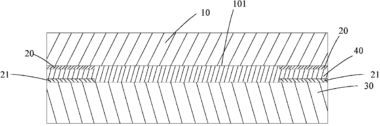
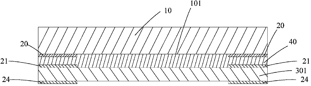
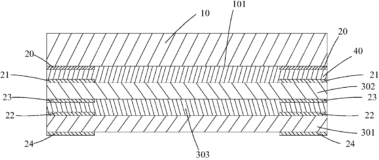
[0030] see figure 1 Shown is a cross-sectional view of the display device of the present invention. The display device and its manufacturing method of the present invention, under the condition that the thickness of the ink remains unchanged, the ink layer is respectively arranged on the surface of each structural layer of the display device, so that the single-layer ink layer can be the thinnest, and the thinnest reaches 5um, which effectively reduces the gap caused by the ink layer. In this way, when OCA optical glue is used for lamination, no air bubbles are guaranteed, and thicker OCA optical glue is not needed. In practice, OCA optical glue can use 50um To realize the lamination between the structural layers, compared with the existing 200um thick optical glue, the optical glue layer is greatly thinned, so that the overall thickness of th...


PUM


Abstract

The invention relates to a display device and a manufacturing method thereof. The display device comprises a display module, a cover plate and an adhesive layer arranged between the display module and the cover plate, wherein a first ink layer is arranged on at least one part between the cover plate and the adhesive layer; the first ink layer is 5-7 microns thick; the display module is provided with a second ink layer. The ink layers are respectively arranged on all structural layers, and the single ink layer is as thin as 5 microns, so that offset generated by the ink layers is greatly reduced; therefore the adhesive layer can adopt a smaller thickness during laminating, and the whole structure of the display device is thinned and can meet requirements of people on light weight and thinness of electronic products; the problem that an optical glue layer is thicker in the prior art is solved.

Description

technical field [0001] The invention relates to the display field, in particular to a display device and a manufacturing method thereof. Background technique [0002] Existing display devices have the following forms, OGS (One Glass Solution, integrated touch) structure, GFF structure (Glass-Flim-Flim, film structure with protective glass), GF structure (Glass-Flim), In-cell structure (the touch sensor function is embedded inside the display screen), and On-cell structure (the touch screen is embedded between the color filter substrate and the polarizer of the display screen). In the above display structure, ink is provided on the back of the touch panel or glass cover, which functions as touch screen insulation, acid resistance, moisture resistance and protection. There are more and more types of ink, and the reliability and reliability are also increasing. it is good. [0003] The ink printing process is very mature. Generally, the ink is printed on the end of the back o...

Claims


Application Information

Patent Timeline
Patent Type & Authority Applications(China)
IPC IPC(8): B32B27/06G06F3/041
CPCB32B7/12B32B37/003B32B37/12B32B37/14B32B38/145B32B2255/20B32B2255/28B32B2264/102B32B2307/4023B32B2307/412B32B2307/422B32B2307/75B32B2457/20F21K2/00
Inventor 马昆良温志伟
Owner EVERDISPLAY OPTRONICS (SHANGHAI) CO LTD
Why Eureka
Try Eureka