A double-ring through-silicon via structure and its manufacturing method

A manufacturing method, ring silicon technology, applied in the direction of semiconductor/solid-state device manufacturing, electrical components, electrical solid-state devices, etc., can solve problems such as lack of shielding signal noise, signal channel coupling, increased crosstalk, and large metal thermal stress, etc., to achieve High frequency signal integrity, improved thermomechanical properties, and reduced thermal stress

Inactive Publication Date: 2017-02-15
XIAN UNIV OF TECH
View PDF3 Cites 0 Cited by
  • Summary
  • Abstract
  • Description
  • Claims
  • Application Information

AI Technical Summary

Problems solved by technology

[0003] However, in the process of making TSVs, TSVs and the entire semiconductor substrate need to undergo many thermal cycles, and the final annealing (275°C) and cooling to room temperature (25°C) process will bring huge damage to the entire structure. Temperature load (-250℃)
Due to the thermal expansion coefficient mismatch between the metal material (especially copper) and the semiconductor substrate, a large thermal stress will be introduced into the silicon substrate around the TSV, which will affect the carrier mobility and device performance and reliability.
On the other hand, with the continuous improvement of integration, the density of through-silicon holes has increased significantly, and the coupling and crosstalk between signal channels have also increased; with the increase of operating frequency of three-dimensional integrated circuits, especially those working in millimeter wave or In the submillimeter wave band, the influence of the parasitic parameters of the TSV itself is enough to submerge the entire signal transmission, seriously affecting the signal integrity of the signal channel
[0004] At present, the existing TSV structure can be divided into four types: cylindrical TSV, tapered TSV, ring TSV and coaxial TSV, among which cylindrical TSV and tapered TSV Due to structural limitations, TSVs and ring-type TSVs do not have the function of shielding signal noise, and are only suitable for low-frequency situations; while coaxial TSVs have superior high-frequency electrical resistance due to the existence of the outer grounding metal ring. Transmission characteristics, but because of the large proportion of metal, it introduces a large thermal stress in the surrounding semiconductor substrate

Method used


Image

  • A double-ring through-silicon via structure and its manufacturing method
  • A double-ring through-silicon via structure and its manufacturing method
  • A double-ring through-silicon via structure and its manufacturing method

Examples


specific Embodiment 1

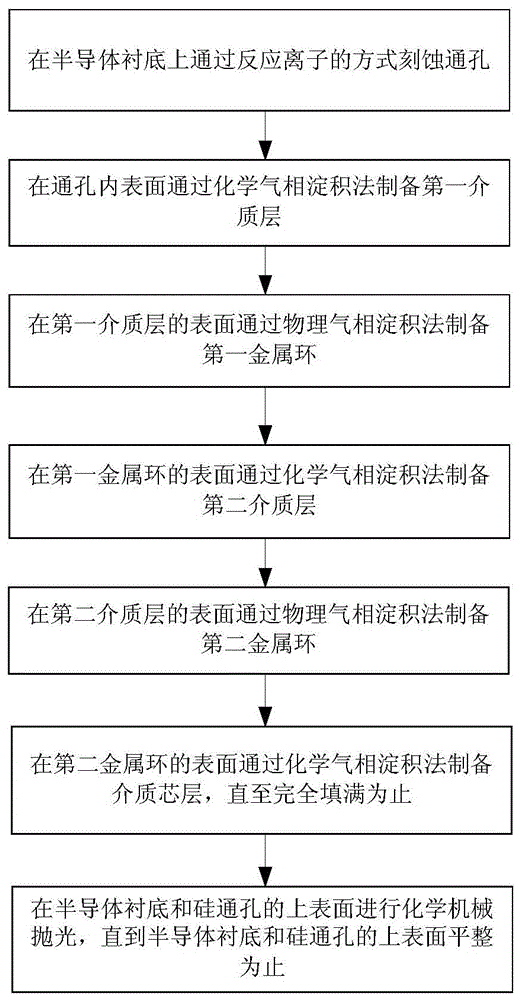
[0036] Such as figure 1 with Figure 3-9 As shown, a method for manufacturing double-ring TSVs includes the following steps:

[0037] (1) On the semiconductor substrate 1, the through hole is etched by means of reactive ions. The semiconductor substrate 1 is a silicon substrate, and its height is 50 μm, and its length and width are 5 mm; the aperture of the through hole is 5.1 μm; step (1 ) The process conditions for reactive ion etching through holes are: use fluoride or chloride gas, decompose fluorine atoms or chlorine atoms in glow discharge, and react with surface silicon atoms to form gaseous products to achieve the purpose of etching; The gas pressure is 15-30 pascals, the reaction gas flow rate is 10-40 ml / min, and the radio frequency power range is 200-350 watts. At the same time, the heat exchanger and the helium cooling technology on the back of the silicon wafer are used for temperature control to ensure that the temperature of the entire silicon wafer is uniform...

specific Embodiment 2

[0054] The preparation process is roughly the same as in Example 1, except that the aperture of the through hole in step (1) is 15 μm;

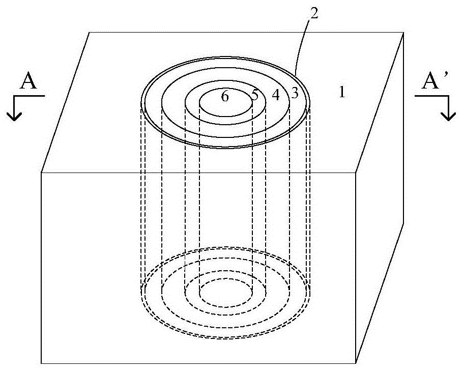
[0055] A double-ring through-silicon via structure, which includes a semiconductor substrate, a first dielectric layer 2, a first metal ring 3, a second dielectric layer 4, a second metal ring 5, and a dielectric core layer 6 from outside to inside.

[0056] The first dielectric layer 2 is a silicon nitride layer, and the thickness of the first dielectric layer 2 is 1 μm;

[0057] The thickness of the first metal ring 3 is 3 μm;

[0058] The second dielectric layer 4 is a silicon nitride layer, and the thickness of the second dielectric layer 4 is 3 μm;

[0059] The thickness of the second metal ring 5 is 3 μm;

[0060] The dielectric core layer 6 is a silicon nitride core layer, and the radius of the dielectric core layer 6 is 5 μm.

[0061] In this embodiment, the semiconductor substrate is a silicon substrate.

[0062] In this embodime...

specific Embodiment 3

[0066] The preparation process is roughly the same as that of Example 1, except that the diameter of the through hole in step (1) is 9.5 μm;

[0067] A double-ring through-silicon via structure, which includes a semiconductor substrate, a first dielectric layer 2, a first metal ring 3, a second dielectric layer 4, a second metal ring 5, and a dielectric core layer 6 from outside to inside.

[0068] The first dielectric layer 2 is a silicon oxynitride layer, and the thickness of the first dielectric layer 2 is 0.5 μm;

[0069] The thickness of the first metal ring 3 is 2 μm;

[0070] The second dielectric layer 4 is a silicon oxynitride layer, and the thickness of the second dielectric layer 4 is 2 μm;

[0071] The thickness of the second metal ring 5 is 2 μm;

[0072] The dielectric core layer 6 is a silicon oxynitride core layer, and the radius of the dielectric core layer 6 is 3 μm.

[0073] In this embodiment, the semiconductor substrate is a silicon substrate.

[0074]...


PUM

PropertyMeasurementUnit
thicknessaaaaaaaaaa
thicknessaaaaaaaaaa
radiusaaaaaaaaaa

Abstract

The invention relates to a double-ring silicon through silicon via structure and a manufacturing method thereof. The double-ring silicon through silicon via structure comprises a semiconductor substrate, a first dielectric layer, a first metal ring, a second dielectric layer, a second metal ring and a dielectric core layer sequentially from outside to inside. The manufacturing method of the double-ring silicon through silicon via structure includes: (1) forming a through via in the semiconductor substrate by etching; (2) preparing the first dielectric layer on the inner surface of the through via; (3) preparing the first metal ring on the surface of the first dielectric layer; (4) preparing the second dielectric layer on the surface of the first metal ring; (5) preparing the second metal ring on the surface of the second dielectric layer; (6) preparing the dielectric core layer on the surface of the second metal ring until fullness is achieved; (7) performing chemical mechanical polishing on the upper surfaces of the semiconductor substrate and the through silicon via. By adoption of the first metal ring which is arranged outside and grounded, a function of shielding noise signals is realized, and high integrity of high-frequency signals is achieved; by adoption of the second metal ring arranged inside, thermal stress is reduced, and thermo-mechanical property is improved.

Description

technical field [0001] The invention belongs to the field of three-dimensional integrated circuits for high-frequency applications, and relates to a through-silicon hole structure and a manufacturing method thereof, in particular to a double-ring through-silicon hole structure and a manufacturing method thereof. Background technique [0002] In the past few decades, the size of microelectronic devices has continued to decrease according to Moore's law, and the performance of electronic products has been improved unprecedentedly. However, after the size of the semiconductor manufacturing process was reduced to 16nm, the process technology gradually reached the physical limit, and small-scale effects such as quantum effects and short-channel effects became more and more prominent, which became the bottleneck for the continued development of Moore's Law. Three-dimensional integrated circuits no longer blindly pursue small size, but use three-dimensional stacking to improve syst...

Claims


Application Information

Patent Timeline
Patent Type & Authority Patents(China)
IPC IPC(8): H01L23/48H01L21/768
Inventor 王凤娟余宁梅
Owner XIAN UNIV OF TECH
Why Eureka
Try Eureka