Integrated nonpolar gan nanowire high electron mobility transistor and its preparation method
A high electron mobility, nanowire technology, applied in the fields of nanotechnology, nanotechnology, semiconductor/solid-state device manufacturing, etc., can solve the problems of uneven distribution of nanowires, low yield, disorder, etc., to solve the problem of uncontrollable The effect of simplification of process steps and optimization of process methods
- Summary
- Abstract
- Description
- Claims
- Application Information
AI Technical Summary
Problems solved by technology
Method used
Image

Examples
preparation example Construction
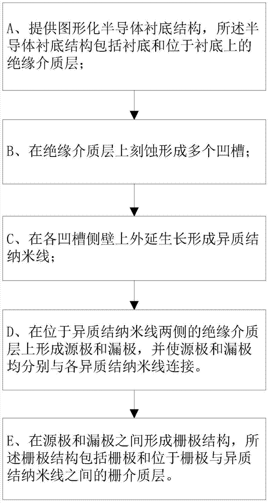
[0041] refer to image 3 , an integrated non-polar GaN nanowire high electron mobility transistor preparation method, comprising the following steps:
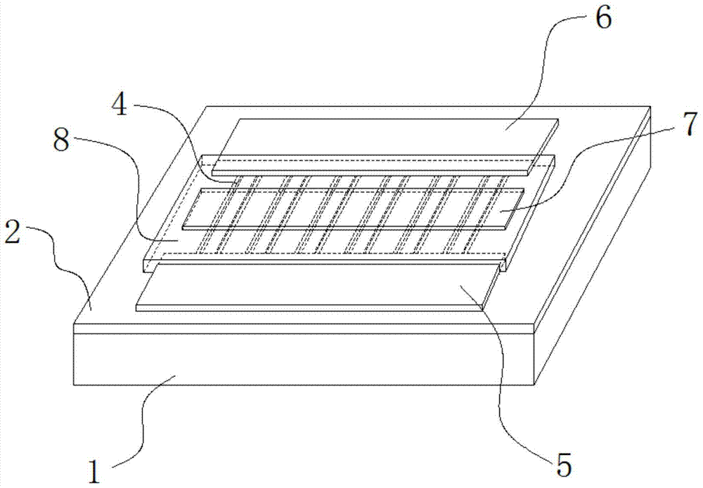
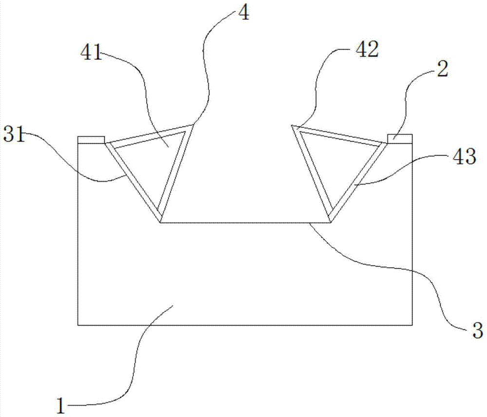
[0042] A. A patterned semiconductor substrate 1 structure is provided, and the semiconductor substrate 1 structure includes a substrate 1 and an insulating dielectric layer 2 positioned on the substrate 1;
[0043] B. Etching and forming a plurality of grooves 3 on the insulating dielectric layer 2;
[0044] C. Epitaxial growth on the sidewalls 31 of each groove 3 to form heterojunction nanowires 4;
[0045] D. Forming a source electrode 5 and a drain electrode 6 on the insulating medium layer 2 located on both sides of the heterojunction nanowire 4, and connecting the source electrode 5 and the drain electrode 6 to each heterojunction nanowire 4;
[0046] E. A gate 7 structure is formed between the source 5 and the drain 6 , the gate 7 structure includes the gate 7 and the gate dielectric layer 8 between the gate 7 and the h...
Embodiment 1
[0054] Embodiment 1, in conjunction with reference Figure 1 ~ Figure 3 Step A is performed to provide a structure of a semiconductor substrate 1 , the structure of the semiconductor substrate 1 includes a substrate 1 and an insulating dielectric layer 2 on the substrate 1 . The material of the substrate 1 is single crystal silicon; the material of the insulating dielectric layer 2 on the substrate 1 is a silicon dioxide layer or silicon nitride, but it is not limited to these two dielectric layers, which can be well known by those skilled in the art. other media layers. The semiconductor substrate 1 is patterned to form an array of rectangular grooves 3 . Wherein forming the rectangular groove 3 of the array comprises: coating photoresist layer on the surface of the silicon dioxide layer; defining the rectangular groove 3 pattern of the array on the photoresist layer; wet etching the silicon dioxide layer; removing the photoresist; wet etching the bottom surface of the groo...
Embodiment 2
[0058] Embodiment 2, in conjunction with reference Figure 1 ~ Figure 3 , to provide a structure of a semiconductor substrate 1 , the structure of the semiconductor substrate 1 includes a substrate 1 and an insulating dielectric layer 2 on the substrate 1 . The material of the substrate 1 is single crystal silicon, and the material of the insulating dielectric layer 2 on the substrate 1 is a silicon dioxide layer or silicon nitride, but it is not limited to these two dielectric layers, which can be known to those skilled in the art. other media layers. The semiconductor substrate 1 is patterned to form an array of rectangular grooves 3 . Wherein forming the rectangular groove 3 of the array comprises: coating photoresist layer on the surface of the silicon dioxide layer; defining the rectangular groove 3 pattern of the array on the photoresist layer; wet etching the silicon dioxide layer; removing the photoresist; wet etching the bottom surface of the groove 3 and the sidewa...
PUM
 Abstract
Description
Claims
Application Information
 - Generate Ideas
- Intellectual Property
- Life Sciences
- Materials
- Tech Scout
- Unparalleled Data Quality
- Higher Quality Content
- 60% Fewer Hallucinations
Browse by: Latest US Patents, China's latest patents, Technical Efficacy Thesaurus, Application Domain, Technology Topic, Popular Technical Reports.
© 2025 PatSnap. All rights reserved.Legal|Privacy policy|Modern Slavery Act Transparency Statement|Sitemap|About US| Contact US: help@patsnap.com