A kind of anti-tritium coating and preparation method thereof
A technology for coating and blocking tritium, applied in coatings, layered products, sputtering, etc., can solve the problems of poor tritium blocking effect and small reduction coefficient of tritium penetration, and achieve excellent performance, reduce tritium penetration channels, high Density effect
- Summary
- Abstract
- Description
- Claims
- Application Information
AI Technical Summary
Problems solved by technology
Method used
Image
Examples
Embodiment 1
[0045] 1) Substrate surface pretreatment: use glow discharge Ar ions to bombard the substrate surface to clean the substrate surface until the substrate surface is cleaned. Among them, the bias voltage is -500~-1000V, and the vacuum is 1.0~1.5Pa.
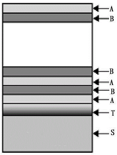
[0046] 2) Depositing the Er transition layer: after cleaning the surface of the substrate in step 1, adjust the argon gas to maintain the vacuum at 0.2-0.5Pa, and apply a pulse bias voltage of -800V to -1500V with a duty ratio of 15% on the substrate, Turn on the target sputtering power supply, and deposit an Er film of about 100 nm, namely the Er transition layer.
[0047] 3) Deposition of Er 2 o 3 Coating: adjust the argon gas so that the vacuum pressure is about 0.5Pa, apply a bias voltage of -90V to the Er transition layer of the substrate, turn on the radio frequency power supply, and deposit a layer of Er2O3 coating with a thickness of 50nm.
[0048] 4) Deposit SiC coating: adjust the argon gas so that the vacuum pressure i...
Embodiment 2~6
[0051] The steps of Examples 2 to 6 are basically the same as those of Example 1, the main difference being that during the coating deposition process, the workpiece bias voltage, vacuum pressure, deposition thickness and number of film layers are different, and the specific parameters are shown in Table 1 below.
[0052] The relevant parameter of table 1 embodiment 1-6
[0053]
PUM
| Property | Measurement | Unit |
|---|---|---|
| thickness | aaaaa | aaaaa |
| thickness | aaaaa | aaaaa |
| thickness | aaaaa | aaaaa |
Abstract
Description
Claims
Application Information
 - Generate Ideas
- Intellectual Property
- Life Sciences
- Materials
- Tech Scout
- Unparalleled Data Quality
- Higher Quality Content
- 60% Fewer Hallucinations
Browse by: Latest US Patents, China's latest patents, Technical Efficacy Thesaurus, Application Domain, Technology Topic, Popular Technical Reports.
© 2025 PatSnap. All rights reserved.Legal|Privacy policy|Modern Slavery Act Transparency Statement|Sitemap|About US| Contact US: help@patsnap.com


