Nano-diamond film with Si-V luminescence and preparation method thereof
A nano-diamond and thin-film technology, which is applied in the direction of nanotechnology, nanotechnology, nanotechnology, etc. for materials and surface science, can solve problems that have not been reported, and achieve the effect of easy operation and simple method
- Summary
- Abstract
- Description
- Claims
- Application Information
AI Technical Summary
Problems solved by technology
Method used
Image
Examples
Embodiment 1
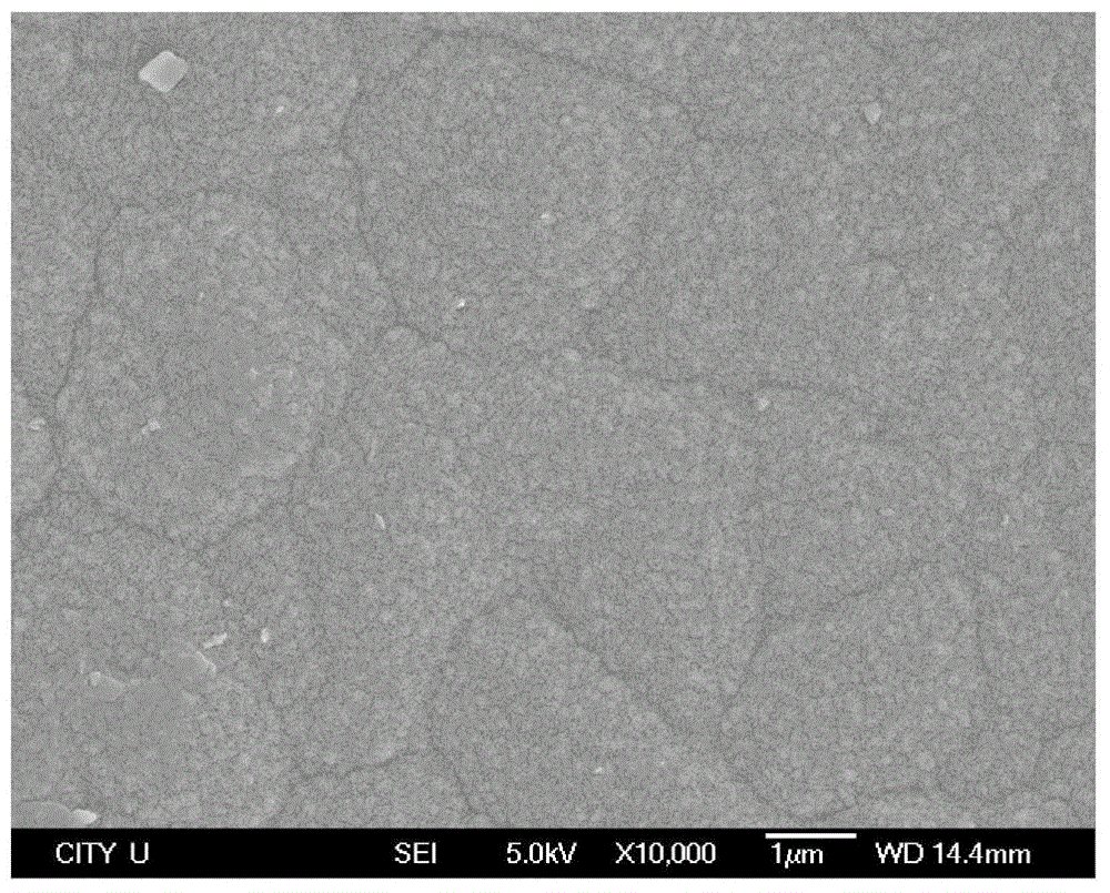
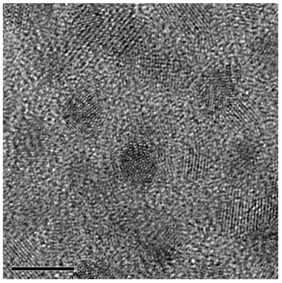
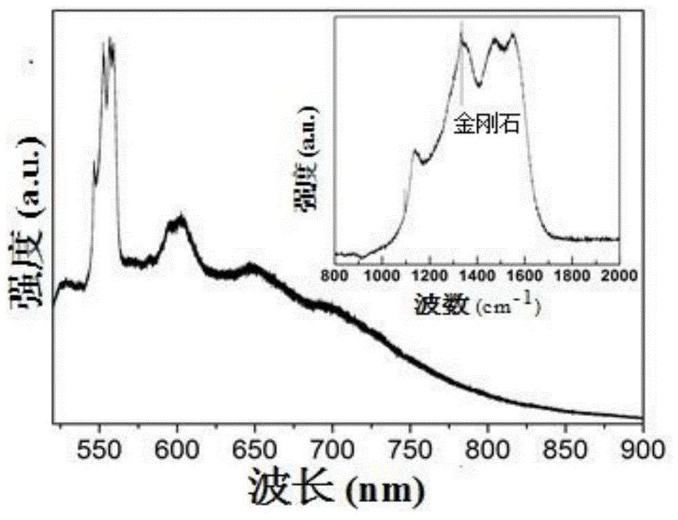
[0028] Polish the monocrystalline silicon wafer with nano-scale diamond powder, and the grinding time is about half an hour. Polished silicon wafers are used as substrates for the growth of nano-diamond films after ultrasonic cleaning. The hot wire chemical vapor deposition method (chemical vapor deposition equipment was purchased from Shanghai Jiaoyou Diamond Coating Co., Ltd.) was used, acetone was used as the carbon source, and acetone was brought into the reaction chamber by hydrogen bubbling. The temperature of the reaction chamber was controlled at 600~ 700° C., the preparation time is 5 hours, and a nano-diamond film with a thickness of 3 μm is prepared. The surface morphology of the film was observed by field emission scanning electron microscopy, and the microstructure of the film was observed by high resolution transmission electron microscope (HRTEM); the luminescent properties of the film were tested by photoluminescence spectroscopy.
[0029] figure 1 It is a fi...
Embodiment 2
[0033]The monocrystalline silicon wafer is polished with nanometer diamond powder, and the polishing time is about half an hour. After the polished silicon wafer is cleaned by an ultrasonic machine, it is used as the substrate for the growth of the nano-diamond film. The hot wire chemical vapor deposition method (chemical vapor deposition equipment was purchased from Shanghai Jiaoyou Diamond Coating Co., Ltd.) was used, acetone was used as the carbon source, and acetone was brought into the reaction chamber by hydrogen bubbling. The temperature of the reaction chamber was controlled at 600~ 700° C., the preparation time is 6 hours, and a nano-diamond film with a thickness of 3.5 μm is prepared. The results of photoluminescence spectroscopy show that the thin film does not have Si-V luminescence peak, indicating that the prepared nano-diamond film does not have Si-V luminescence properties.
[0034] The above-mentioned nano-diamond film was incubated in the air at 600°C for 30...
Embodiment 3
[0037] The monocrystalline silicon wafer is polished with nanometer diamond powder, and the polishing time is about half an hour. After the polished silicon wafer is cleaned by an ultrasonic machine, it is used as the substrate for the growth of the nano-diamond film. The hot wire chemical vapor deposition method (chemical vapor deposition equipment was purchased from Shanghai Jiaoyou Diamond Coating Co., Ltd.) was used, acetone was used as the carbon source, and acetone was brought into the reaction chamber by hydrogen bubbling. The temperature of the reaction chamber was controlled at 600~ 700° C., the preparation time is 5 hours, and a nano-diamond film with a thickness of 3 μm is prepared. The results of photoluminescence spectroscopy show that the thin film does not have Si-V luminescence peak, indicating that the prepared nano-diamond film does not have Si-V luminescence properties.
[0038] The above-mentioned nano-diamond film was incubated in the air at 700°C for 5 m...
PUM
| Property | Measurement | Unit |
|---|---|---|
| thickness | aaaaa | aaaaa |
| diameter | aaaaa | aaaaa |
Abstract
Description
Claims
Application Information
 - R&D
- Intellectual Property
- Life Sciences
- Materials
- Tech Scout
- Unparalleled Data Quality
- Higher Quality Content
- 60% Fewer Hallucinations
Browse by: Latest US Patents, China's latest patents, Technical Efficacy Thesaurus, Application Domain, Technology Topic, Popular Technical Reports.
© 2025 PatSnap. All rights reserved.Legal|Privacy policy|Modern Slavery Act Transparency Statement|Sitemap|About US| Contact US: help@patsnap.com


