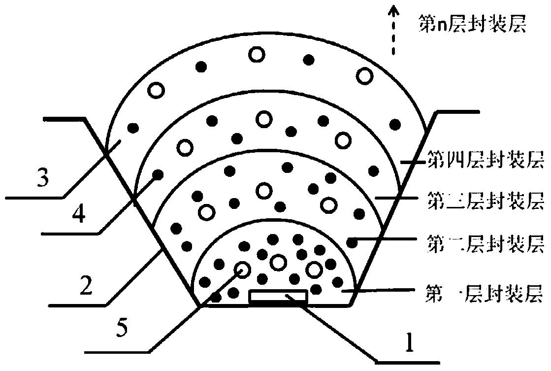
Multi-layer white light LED (Light Emitting Diode) device with gradient refractive indexes and packaging method thereof
A LED device, gradient refractive index technology, applied in semiconductor devices, electrical components, circuits, etc., can solve the problems of unable to meet the requirements of the amount of fluorescent conversion materials, difficult application of high-power devices, limited production of quantum dots, etc., to achieve luminous efficiency Good thermal stability and luminescence, high production efficiency, and the effect of reducing production efficiency
- Summary
- Abstract
- Description
- Claims
- Application Information
AI Technical Summary
Problems solved by technology
Method used
Image
Examples
Embodiment 1
[0044] Embodiment 1: adopt nanometer SiO 2 Scattering agent-encapsulated single-layer structure white LED device
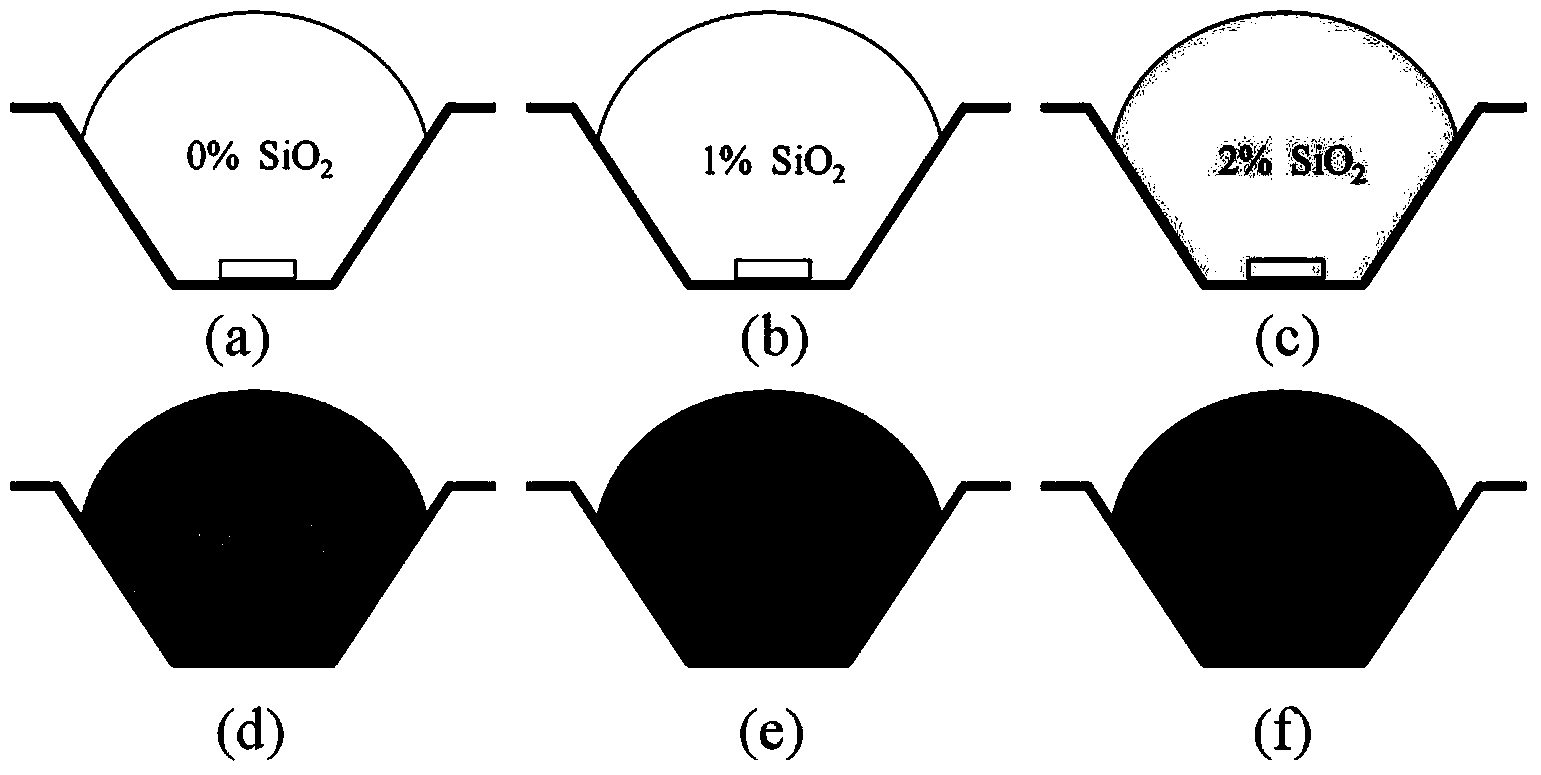
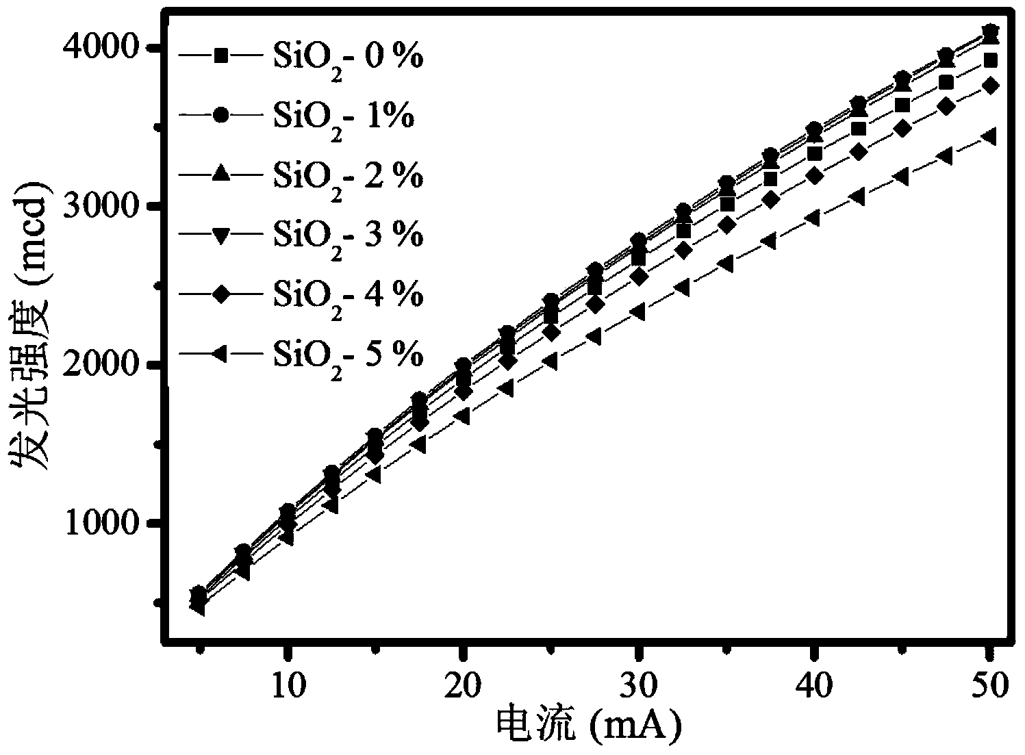
[0045] First use nano-SiO 2 As a scattering agent, it is used to encapsulate single-layer structure white LED devices. SiO 2 The mass ratio of the encapsulating glue in the layer where it is located is set to 0, 1%, 2%, 3%, 4% and 5% respectively. The phosphor powder accounts for 13% by mass of the encapsulating glue in the layer where it is located (the same applies to the following embodiments).
[0046] nano-SiO 2 JY100-01 hydrophobic nano-SiO produced by Anhui Jingye Nano Technology Co., Ltd. 2 , its particle size ≤ 25nm, BET specific surface 170 ± 20, SiO 2 Purity ≥ 99.5%; fluorescent material adopts YBO from Foshan Nanhai Langda Fluorescent Material Co., Ltd. 4 Type YAG: Ce yellow phosphor, its refractive index is 1.823, and its specific gravity is 4.3; the blue LED chip adopts the semi-finished product after solid crystal and wire bonding of Guangdon...
Embodiment 2
[0051] Embodiment 2: adopt nano-SiO 2 Scattering agent encapsulation two-layer structure white light LED device
[0052] This embodiment utilizes nano-SiO 2 As a scattering agent, adopt the same process as in Example 1, and package such as Figure 5 The two-layer structure white LED device shown, its relative luminous intensity varies with the current as Figure 6 shown. It can be seen from the figure that with and without adding nano-SiO 2 Compared with the single-layer packaging structure, except 2% (first layer)-1% (second layer, the following is similar) ( Figure 5 (f)) and 2%-0.5% ( Figure 5 (e)), the luminous intensity of other white LED devices using two-layer structure has been improved, and the highest luminous intensity is 0.5%-0% ( Figure 5 (a)) two-layer structure; followed by 1%-0% ( Figure 5 (b)) and 2%-0% ( Figure 5 (c)) White LEDs with two-layer structure have similar luminous intensity. The luminous intensity of white LEDs with these three struct...
Embodiment 3
[0053] Embodiment 3: adopt nano-SiO 2 White light LED device with three-layer structure encapsulated by scattering agent
[0054]This embodiment utilizes nano-SiO 2 As a scattering agent, adopt the same process as in Example 1, and package such as Figure 7 The three-layer structure white LED device shown, its relative luminous intensity varies with the current as Figure 8 shown. All white LED devices packaged with a three-layer structure were better than those without adding nano-SiO 2 The luminous intensity of single-layer structure LED is high, but it is better than nano-SiO 2 The luminous intensity of the single-layer structure LED with the addition amount of 1% is weak. Using nano-SiO 2 In the three-layer structure of the scattering agent, the highest luminous intensity is 2% (first layer)-1% (second layer)-0% (third layer) ( Figure 7 (a)). In addition, the greater the driving current, the greater the relative luminous intensity, which is still very obvious for ...
PUM
 Abstract
Description
Claims
Application Information
 - R&D
- Intellectual Property
- Life Sciences
- Materials
- Tech Scout
- Unparalleled Data Quality
- Higher Quality Content
- 60% Fewer Hallucinations
Browse by: Latest US Patents, China's latest patents, Technical Efficacy Thesaurus, Application Domain, Technology Topic, Popular Technical Reports.
© 2025 PatSnap. All rights reserved.Legal|Privacy policy|Modern Slavery Act Transparency Statement|Sitemap|About US| Contact US: help@patsnap.com


