Wet etching chemical transfer method for enhancing surface cleanliness of graphene
A graphene surface, wet etching technology, applied in chemical instruments and methods, inorganic chemistry, carbon compounds, etc., can solve problems such as introducing surface states, and achieve the effect of improving cleanliness
- Summary
- Abstract
- Description
- Claims
- Application Information
AI Technical Summary
Problems solved by technology
Method used
Image
Examples
Embodiment 1
[0023] (1) A continuous graphene film grown on a Cu catalytic substrate ( figure 1 (a)) Deposit a layer of metal film on the surface, and the metal film is one or two, three or even seven alloys of Al, Zn, Fe, Co, Ni, Mo or Cu, and the thickness of the metal layer is 10-1000nm, the preferred thickness of the Al film is 30-100nm; then the preferred recommended surface deposition of a metal Al film layer of PMMA with a thickness of 100-500nm, the preferred thickness is 150-250nm; a layer of 200nm is spin-coated on the surface of the Al film thick polymethyl methacrylate (PMMA) (such as figure 1 (b));
[0024] (2) Put the PMMA / Al / graphene / Cu sample into FeCl 3 On the liquid surface of the etching solution, the PMMA faces upward, and after the Cu is completely etched away, the PMMA / Al / graphene combination is transferred to the Si / SiO 2 on the target substrate (e.g. figure 1 (c));
[0025] (3) Then PMMA / Al / graphene / Si / SiO 2 The combination is immersed in 40-70°C acetone solut...
Embodiment 2
[0029] (1) Deposit a layer of 30nm thick Al film on the surface of the continuous graphene film grown on the Ni catalyst substrate; then spin-coat polymethylmethacrylate (PMMA) with a thickness of 200nm on the surface of the Al film;
[0030] (2) Put the PMMA / Al / graphene / Cu sample into FeCl 3 On the liquid surface of the etching solution, the PMMA faces upwards. After the Cu is completely etched away, the PMMA / Al / graphene sample is transferred to the target substrate Si / SiO 2 on the substrate;
[0031] (3) PMMA / Al / graphene / Si / SiO 2 Samples were immersed in acetone solution at 50°C for 2 hours to remove PMMA;
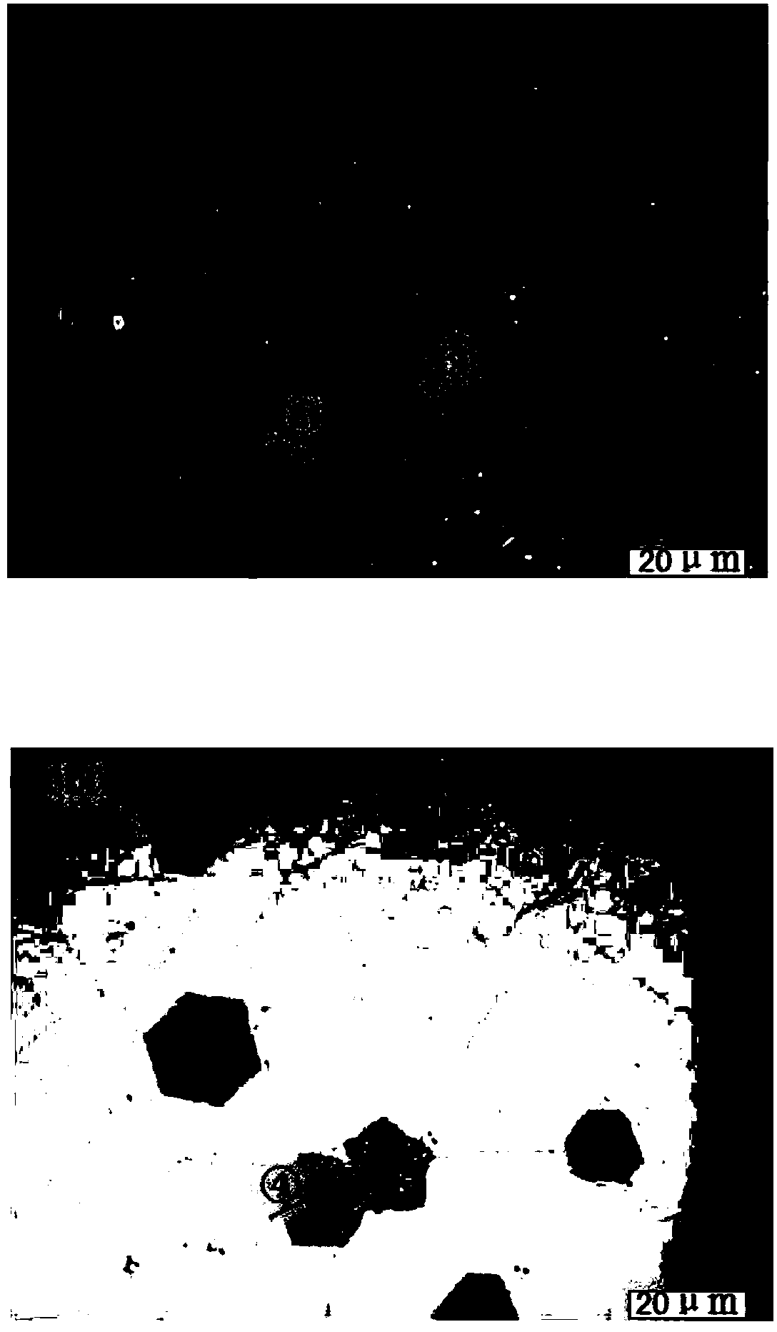
[0032] (4) Finally Al / graphene / Si / SiO 2 Sample immersion into HNO 3 or FeCl 3 Metal Al is removed from the solution to obtain a transferred continuous graphene film. The result is as figure 2 (b) shown.
Embodiment 3
[0034] (1) Deposit a layer of 30nm thick Al film on the surface of single crystal graphene grown on the Cu catalyst substrate; then spin-coat polymethylmethacrylate (PMMA) with a layer of 200nm thickness on the Al film;
[0035] (2) Put the PMMA / Al / graphene / Cu sample into FeCl 3 On the liquid surface of the etching solution, the PMMA faces upwards. After the Cu is completely etched away, the PMMA / Al / graphene sample is transferred to the Si / SiO 2on the substrate;
[0036] (3) PMMA / Al / graphene / Si / SiO 2 The sample was immersed in acetone solution at 50°C for 2 hours to remove PMMA;
[0037] (4) Finally Al / graphene / Si / SiO 2 Sample immersion into HNO 3 or FeCl 3 Metal Al is removed from the solution to obtain a transferred continuous graphene film. The result is as figure 2 (b) shown.
[0038] Experimental results prove that the method of the present invention is effective and can improve the cleanliness of the graphene surface.
PUM
| Property | Measurement | Unit |
|---|---|---|
| Thickness | aaaaa | aaaaa |
| Thickness | aaaaa | aaaaa |
Abstract
Description
Claims
Application Information
 - R&D Engineer
- R&D Manager
- IP Professional
- Industry Leading Data Capabilities
- Powerful AI technology
- Patent DNA Extraction
Browse by: Latest US Patents, China's latest patents, Technical Efficacy Thesaurus, Application Domain, Technology Topic, Popular Technical Reports.
© 2024 PatSnap. All rights reserved.Legal|Privacy policy|Modern Slavery Act Transparency Statement|Sitemap|About US| Contact US: help@patsnap.com


