Detection method for repeated position defects in batch of wafers

A wafer batch and detection method technology, applied in the direction of semiconductor/solid-state device testing/measurement, electrical components, circuits, etc., can solve problems such as complex operation, defects at the same position in lithography, and difficult to identify circuit defects without consideration, to achieve The effect of reducing the possibility of misjudgment

Inactive Publication Date: 2014-09-03
SHANGHAI HUALI MICROELECTRONICS CORP
View PDF6 Cites 23 Cited by
  • Summary
  • Abstract
  • Description
  • Claims
  • Application Information

AI Technical Summary

Problems solved by technology

[0004] The method of this patent improves the accuracy of defect detection, but the operation is more complicated, and it does not consider the circuit defects that are more difficult to identify and randomly distributed, and defects may be caused at the same position of the chip due to problems such as photolithography.

Method used


Image

  • Detection method for repeated position defects in batch of wafers
  • Detection method for repeated position defects in batch of wafers
  • Detection method for repeated position defects in batch of wafers

Examples


Embodiment Construction

[0036] The present invention provides a high-sensitivity detection method for repeated position defects, which can be applied to processes with technical nodes of 90nm, 65 / 55nm, 45 / 40nm, 32 / 28nm, 130nm or more and 22nm or less; and can be applied to the following Technology platforms: Logic, Memory, RF, HV, Analog / Power, MEMS, CIS, Flash and eFlash.

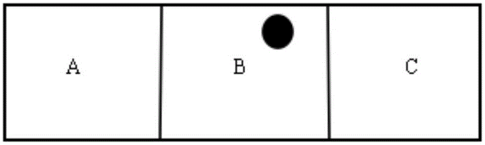
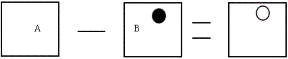
[0037] Such as Figure 6-10 As shown, the present invention is a method for detecting repeated position defects in a wafer batch, and the method includes:

[0038] Step S1: Provide a batch of wafers for defect detection, and establish the same coordinate system on each of the wafers;

[0039] Step S2: Obtain all defect positions on each of the wafers, and obtain corresponding defect coordinates according to the coordinate system;

[0040] Step S3, comparing the coordinate of the defect on any one of the wafers with the coordinate of the defect on each of the other wafers, so as to mark the coordinate of the defect that is repeated at lea...


PUM


Abstract

The invention discloses a detection method for repeated position defects in a batch of wafers. The method comprises the steps that the batch of wafers which needs defect detection is provided, and all the wafers are provided with identical coordinate systems; all defect positions of each wafer are obtained, and corresponding defect coordinates are obtained according to the coordinate system; a random defect coordinate of the wafer is compared with defect coordinates of all the other wafers to mark defect coordinates which are repeated for at least one time as repeated defect coordinates; and according to all the repeated defect coordinates , a simulated defect distribution map is generated. The method can be used to clearly identify repeated circuit defects, and the possibility of engineering determination errors is greatly reduced.

Description

Technical field [0001] The invention relates to the technical field of detection of circuit defects, in particular to a detection method of repeated position defects in a wafer batch. Background technique [0002] In the current technical field, with the development of integrated circuit technology and the continuous reduction of feature size, the distribution of circuits on the chip is becoming more and more complicated. A small error in any link will cause the failure of the entire product, so the process control The requirements are getting stricter. In order to detect product defects in time, semiconductors generally configure corresponding defect detection equipment to detect defects in the product. Therefore, in the production process, in order to find and solve problems in time, optical and electronic defect detection equipment are equipped to detect products online. Whether it is optical or electronic defect detection, the basic principle of its work is to obtain several...

Claims


Application Information

Patent Timeline
IPC IPC(8): H01L21/66
CPCH01L22/12
Inventor 倪棋梁范荣伟陈宏璘龙吟
Owner SHANGHAI HUALI MICROELECTRONICS CORP
Why Eureka
Try Eureka