Method for preparing micro-nano textures through ultrasonic vibration

An ultrasonic vibration, micro-nano technology, applied in the manufacture of micro-structure devices, micro-structure technology, micro-structure devices, etc., can solve the problem that mask lithography cannot achieve size control, scanning probe processing efficiency is low, and equipment is expensive. Surface and other problems, to achieve the effect of reducing the time for making masks, less stress, and better surface quality

Inactive Publication Date: 2014-08-20
CHINA UNIV OF MINING & TECH
View PDF4 Cites 7 Cited by
  • Summary
  • Abstract
  • Description
  • Claims
  • Application Information

AI Technical Summary

Problems solved by technology

At present, the processing methods commonly used to texture the surface of single crystal silicon include high-energy beam direct writing, scanning probe processing, nanoimprinting and mask lithography, etc., but they all have certain defects, such as high-energy beam direct writing equipment is expensive And the surface of the prepared texture is rough; the processing efficiency of scanning probe is low and it is difficult to realize large-area processing; mask lithography cannot realize the preparation of size-controllable and large-area micro-nano texture

Method used


Image

  • Method for preparing micro-nano textures through ultrasonic vibration
  • Method for preparing micro-nano textures through ultrasonic vibration

Examples


Embodiment 1

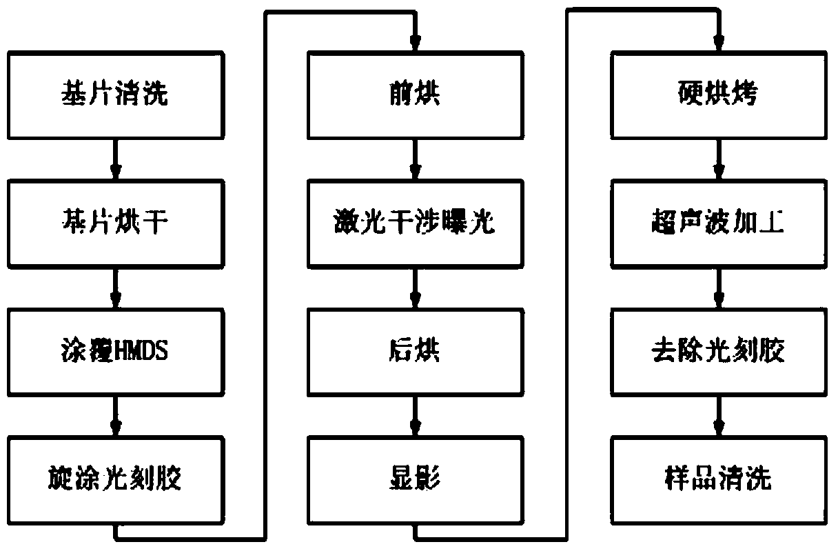
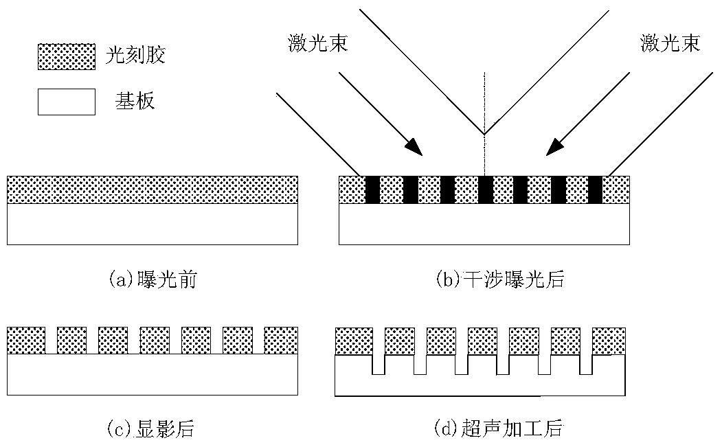
[0024] Embodiment 1: In this method, firstly, a layer of photoresist is evenly coated on the surface of the substrate by using a coater; the substrate with photoresist is subjected to interference exposure in a laser interference system to realize texturing of the photoresist processing; finally, the substrate is placed in an ultrasonic processing system for processing, and the substrate material in the non-photoresist-covered area will be removed. As the ultrasonic processing time increases, the removal depth will gradually increase. By controlling the exposure of laser interference lithography parameters and ultrasonic vibration processing parameters to achieve size-controllable and large-area periodic micro-nano texture preparation.

[0025] The preparation method of the micro-nano texture in the present invention adopts the processing method of laser interference photolithography and ultrasonic vibration.

[0026] Process flow of the present invention is:

[0027] First, ...


PUM


Abstract

The invention discloses a method for preparing micro-nano textures through ultrasonic vibration and belongs to a preparation method of silicon surface micro-nano textures. The method comprises the following steps: firstly, uniformly coating a layer of photo-etching glue on the surface of a substrate by using a glue homogenizer; then carrying out interferential exposure on the substrate with the photo-etching glue in a laser interferometer system to realize texturing treatment on the photo-etching glue; and finally machining the substrate in an ultrasonic machining system, removing the substrate material in an area which is not covered by the photo-etching glue, gradually increasing the removal depth along with the increase of the ultrasonic machining time, controlling exposure parameters of laser interference photo-etching and ultrasonic vibration machining parameters to prepare periodic micro-nano textures which are controllable in size and large in area. The method for preparing the micro-nano textures through ultrasonic vibration has the advantages that the method is pollution-free due to the adoption of ultrasonic vibration machining, simple to operate, free of damage to the photo-etching glue layer on the surface of the substrate and good in pattern transfer effect; by changing the size of a vibration tool, different areas can be machined; by means of the ultrasonic vibration, the machining accuracy is high and the surface quality is good; the substrate is relatively small in stress in the machining process.

Description

technical field [0001] The invention relates to a method for preparing a size-controllable, large-area periodic micro-nano texture, especially a method for preparing a micro-nano texture by ultrasonic vibration. technical background [0002] Micro-Electro-Mechanical Systems (MEMS) gradually occupy an important position in the fields of digital communication, medical treatment, environmental engineering, aerospace, industry, weapons and sensor technology due to its advantages of light weight, small size and low energy consumption. Monocrystalline silicon has excellent mechanical and physical properties, and has good compatibility with microelectronic integrated circuit technology, and is the main structural material in M / NEMS. Micro-nano textures can effectively improve the surface properties of materials. Therefore, the preparation of micro-nano textures on silicon surfaces has become a research hotspot at home and abroad in recent years. At present, the processing methods ...

Claims


Application Information

Patent Timeline
Patent Type & Authority Applications(China)
IPC IPC(8): B81C1/00
Inventor 杨海峰贺海东唐玮杨建华郝敬宾朱华
Owner CHINA UNIV OF MINING & TECH
Why Eureka
Try Eureka