ESD countermeasures
A technology of components and electrostatics, applied in the field of electrostatic response components, to achieve the effects of small electrostatic capacitance, suppression of short-circuit damage or peak voltage, short-circuit rate or excellent durability
- Summary
- Abstract
- Description
- Claims
- Application Information
AI Technical Summary
Problems solved by technology
Method used
Image
Examples
no. 1 Embodiment approach
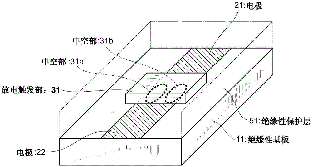
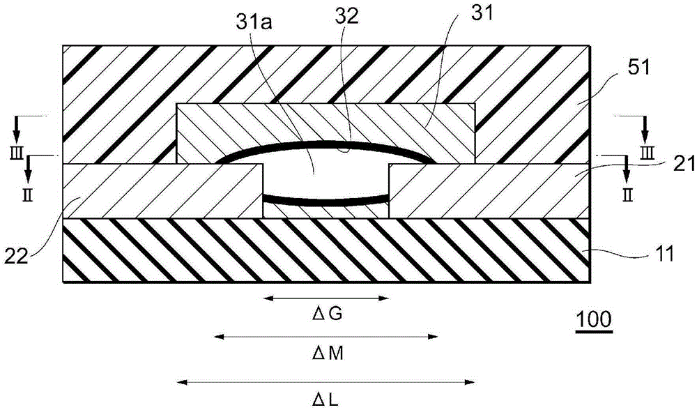
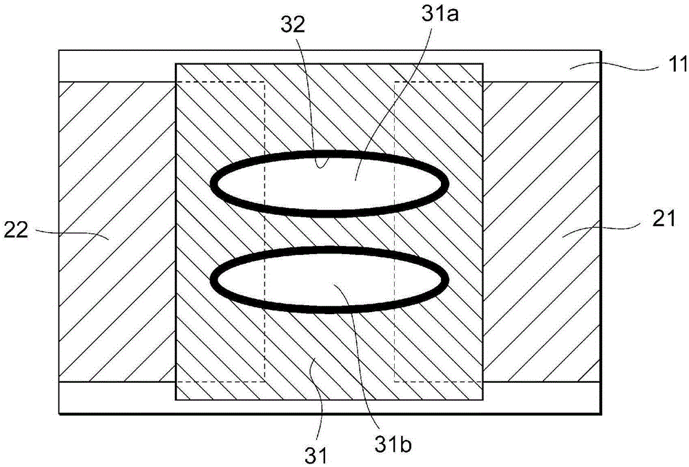
[0060] figure 1 It is a schematic perspective view schematically showing the electrostatic countermeasure device of this embodiment. figure 2 It is a schematic cross-sectional view schematically showing the electrostatic countermeasure device of this embodiment. image 3 yes figure 2 The II-II line sectional view in.
[0061] The electrostatic countermeasure device 100 includes an insulating substrate 11, a pair of electrodes 21 and 22 arranged on the insulating substrate 11, a discharge triggering part 31 arranged between these electrodes 21 and 22, and a device electrically connected to the electrodes 21 and 22. Terminal electrode 41 (refer to Figure 8 ), and an insulating protective layer 51 formed to cover the discharge triggering portion 31. The discharge inducing part 31 has a structure in which minute voids are dispersed discontinuously, and has a hollow structure having at least one hollow part 31a, 31b. Here, the pair of electrodes 21, 22 is arranged such that...
Embodiment 1
[0087] First, if Figure 6 As shown, the preparation will consist of a principal component of Al 2 o 3 A green sheet obtained by thinning a material composed of a glass component is used as an insulating substrate 11 . On the one insulating surface 11 a , Ag paste was printed by screen printing so as to have a thickness of 0.2 μm, thereby patterning a pair of strip-shaped electrodes 21 and 22 arranged facing each other. For a pair of printed electrodes, the length of the electrodes 21 and 22 is 0.5 mm, the width is 0.4 mm, and the gap distance ΔG between the electrodes 21 and 22 is 40 μm.
[0088] Below, such as Figure 7 As shown, the discharge triggering portion 31 is formed on the insulating substrate 11 and the electrodes 21 and 22 in the following order.
[0089] First, let SiO as the insulating inorganic material 34 2 Glass particles (manufactured by Nippon Yamamura Glass Co., Ltd., product serial number: ME13) as the main component are 10 vol%, and Al as the insula...
Embodiment 2
[0094] Except for the screen printing of the paste-like mixture for forming the hollow part, only one part is screen-printed in an ellipsoidal shape, and the same operation as in Example 1 is carried out to produce a structure composed of micro-voids 35 discontinuously scattered. And it has the discharge trigger part 31 of a hollow structure which has one hollow part 31a, and the electrostatic countermeasure device 100 of Example 2 was obtained.
PUM
 Abstract
Description
Claims
Application Information
 - R&D
- Intellectual Property
- Life Sciences
- Materials
- Tech Scout
- Unparalleled Data Quality
- Higher Quality Content
- 60% Fewer Hallucinations
Browse by: Latest US Patents, China's latest patents, Technical Efficacy Thesaurus, Application Domain, Technology Topic, Popular Technical Reports.
© 2025 PatSnap. All rights reserved.Legal|Privacy policy|Modern Slavery Act Transparency Statement|Sitemap|About US| Contact US: help@patsnap.com


