Multilayer Ceramic Capacitors
A technology of laminated ceramics and capacitors, which is applied in the direction of laminated capacitors, fixed capacitor electrodes, fixed capacitor dielectrics, etc., can solve the problems that are difficult to meet the needs of miniaturization and large capacitance, and achieve miniaturization and large capacitance, Effect of reducing mechanical strain and suppressing vibration
- Summary
- Abstract
- Description
- Claims
- Application Information
AI Technical Summary
Problems solved by technology
Method used
Image
Examples
no. 1 approach 》
[0070]
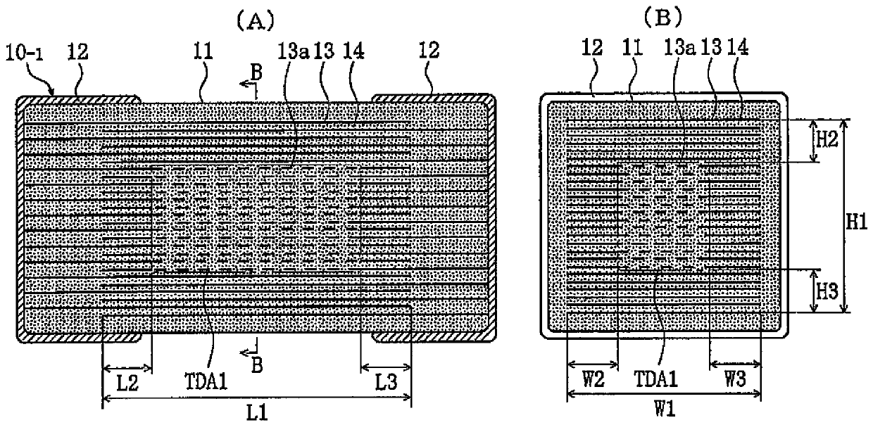
[0071] First, the structure of multilayer ceramic capacitor 10-1 will be described. figure 1 (A) and figure 1 The multilayer ceramic capacitor 10-1 shown in (B) includes: a capacitor body 11 having a substantially cuboid shape, and the reference dimensions of length, width, and height have a relationship of length>width=height, or a relationship of length>width>height; and A pair of external electrodes 12 are provided at both ends in the longitudinal direction of the capacitor body 11 .
[0072] Capacitor body 11 has a structure in which 26 internal electrode layers 13 are laminated with dielectric layer 14 interposed therebetween, and there are boundaries (unsigned) where only dielectric layer 14 is laminated on the upper and lower sides in the height direction. The actual number of internal electrode layers in an actual laminated ceramic capacitor to cope with miniaturization and increase in capacitance is 100 or more. However, since there is also a relationship ...
no. 2 approach 》
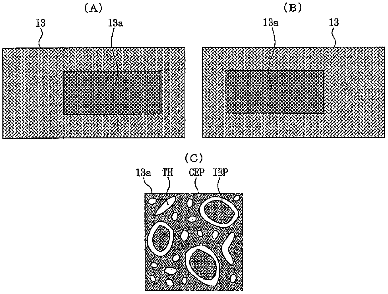
[0093] First, the structure of multilayer ceramic capacitor 10-2 will be described. Figure 5 (A), and Figure 5 The multilayer ceramic capacitor 10-2 shown in (B) is structurally different from the multilayer ceramic capacitor 10-1 of the first embodiment as follows: Figure 5 As shown, among the 26 internal electrode layers 13, the 14-layer internal electrode layer 13 existing in the center of the lamination direction has the following second All parts 13b of the electrode part are isolated.
[0094] Image 6 (A) shows the 14-layer internal electrode layer 13 including all parts 13a of the first isolated electrode part and all parts 13b of the second isolated electrode part. Figure 5 The upper surface of the internal electrode layer 13 of the odd-numbered layer from the top, Image 6 (B) shows that in the 14-layer internal electrode layer 13 Figure 5 The upper surface of the internal electrode layer 13 of the even-numbered layer from the top. From these figures, it c...
PUM
| Property | Measurement | Unit |
|---|---|---|
| thickness | aaaaa | aaaaa |
| thickness | aaaaa | aaaaa |
Abstract
Description
Claims
Application Information
 - R&D
- Intellectual Property
- Life Sciences
- Materials
- Tech Scout
- Unparalleled Data Quality
- Higher Quality Content
- 60% Fewer Hallucinations
Browse by: Latest US Patents, China's latest patents, Technical Efficacy Thesaurus, Application Domain, Technology Topic, Popular Technical Reports.
© 2025 PatSnap. All rights reserved.Legal|Privacy policy|Modern Slavery Act Transparency Statement|Sitemap|About US| Contact US: help@patsnap.com


