Method of manufacturing photoelectric conversion device
A photoelectric conversion device and manufacturing method technology, applied in photovoltaic power generation, final product manufacturing, sustainable manufacturing/processing, etc., can solve the space limitation of the number of film-forming chambers, the complex and expensive mechanism of substrate movement, and the mechanical structure of the intermediate chamber Complicated and other issues, to achieve good photoelectric conversion characteristics and low cost effects
- Summary
- Abstract
- Description
- Claims
- Application Information
AI Technical Summary
Problems solved by technology
Method used
Image
Examples
no. 1 approach
[0051]
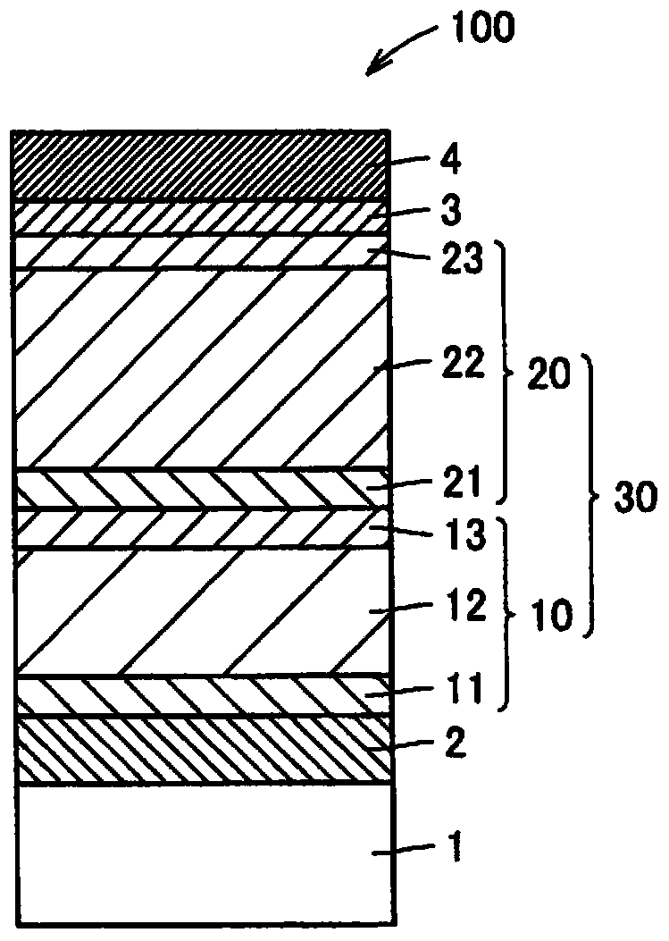
[0052] image 3 is a cross-sectional view schematically showing the structure of a photoelectric conversion device manufactured by the manufacturing method of this embodiment. image 3 The photoelectric conversion device 100 shown has a first photoelectric converter 10 , a second photoelectric converter 20 , a conductive film 3 and a metal electrode 4 on a transparent conductive film 2 formed on a substrate 1 . The first photoelectric converter 10 is an amorphous pin structure laminate formed by sequentially laminating the first p-type semiconductor layer 11, the i-type amorphous silicon-based photoelectric conversion layer 12, and the first n-type semiconductor layer 13. The converter 20 is a microcrystalline pin structure laminate in which a second p-type semiconductor layer 21 , an i-type microcrystalline silicon-based photoelectric conversion layer 22 , and a second n-type semiconductor layer 23 are sequentially laminated. In the present specification, "microcr...
Embodiment 1a
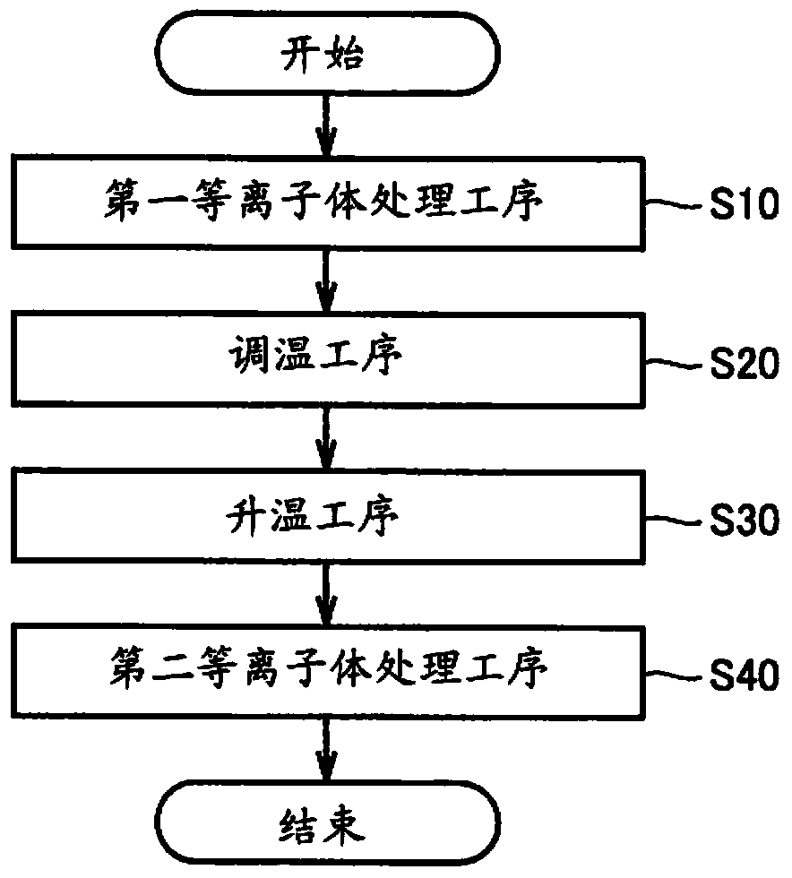
[0067] In the manufacturing method of this embodiment, the power density of the unit electrode in the first plasma treatment step (S10) is set to 0.068 W / cm 2 , the power density of the unit electrode in the second plasma treatment process (S40) is set to 0.225W / cm 2 , thus fabricating a photoelectric conversion device.
[0068] Figure 4 It is a graph showing the change of the control temperature and the actual processing temperature from the 1st plasma processing process (S10) to the 2nd plasma processing process (S40) in this Example. exist Figure 4 In , the horizontal axis represents time, and the vertical axis represents temperature. exist Figure 4 In , the dotted line represents the control temperature, and the solid line represents the actual treatment temperature. The process temperature, ie the temperature of the anode, was measured by thermocouples.
[0069] like Figure 4 As shown, in the first plasma processing step (S10), the control temperature is set to...
Embodiment 1b
[0072] In the manufacturing method of this embodiment, the power density of the unit electrode in the first plasma treatment step (S10) is set to 0.068 W / cm 2 , the power density of the unit electrode in the second plasma treatment process (S40) is set to 0.300W / cm 2 , thus fabricating a photoelectric conversion device.
[0073] Figure 5 It is a graph showing the change of the control temperature and processing temperature from the 1st plasma processing process (S10) to the 2nd plasma processing process (S40) in this Example. exist Figure 5 In , the dotted line represents the control temperature, and the solid line represents the actual treatment temperature. The process temperature, ie the temperature of the anode, was measured by thermocouples.
[0074] like Figure 5 As shown, in the second plasma processing step (S40), the power density is relatively high, and the substrate is easy to be heated by high-frequency discharge, and the processing temperature continues to...
PUM
 Abstract
Description
Claims
Application Information
 - R&D
- Intellectual Property
- Life Sciences
- Materials
- Tech Scout
- Unparalleled Data Quality
- Higher Quality Content
- 60% Fewer Hallucinations
Browse by: Latest US Patents, China's latest patents, Technical Efficacy Thesaurus, Application Domain, Technology Topic, Popular Technical Reports.
© 2025 PatSnap. All rights reserved.Legal|Privacy policy|Modern Slavery Act Transparency Statement|Sitemap|About US| Contact US: help@patsnap.com


