Active Matrix Image Sensing Panel and Device
An image sensing and active matrix technology, applied in radiation control devices, etc., can solve problems such as sensing distortion, source leakage, potential difference rise, etc., and achieve the effect of avoiding image sensing distortion and increasing critical voltage
- Summary
- Abstract
- Description
- Claims
- Application Information
AI Technical Summary
Problems solved by technology
Method used
Image
Examples
Embodiment Construction
[0049] The active matrix image sensing panel and device according to preferred embodiments of the present invention will be described below with reference to related drawings, wherein the same elements will be described with the same reference symbols.
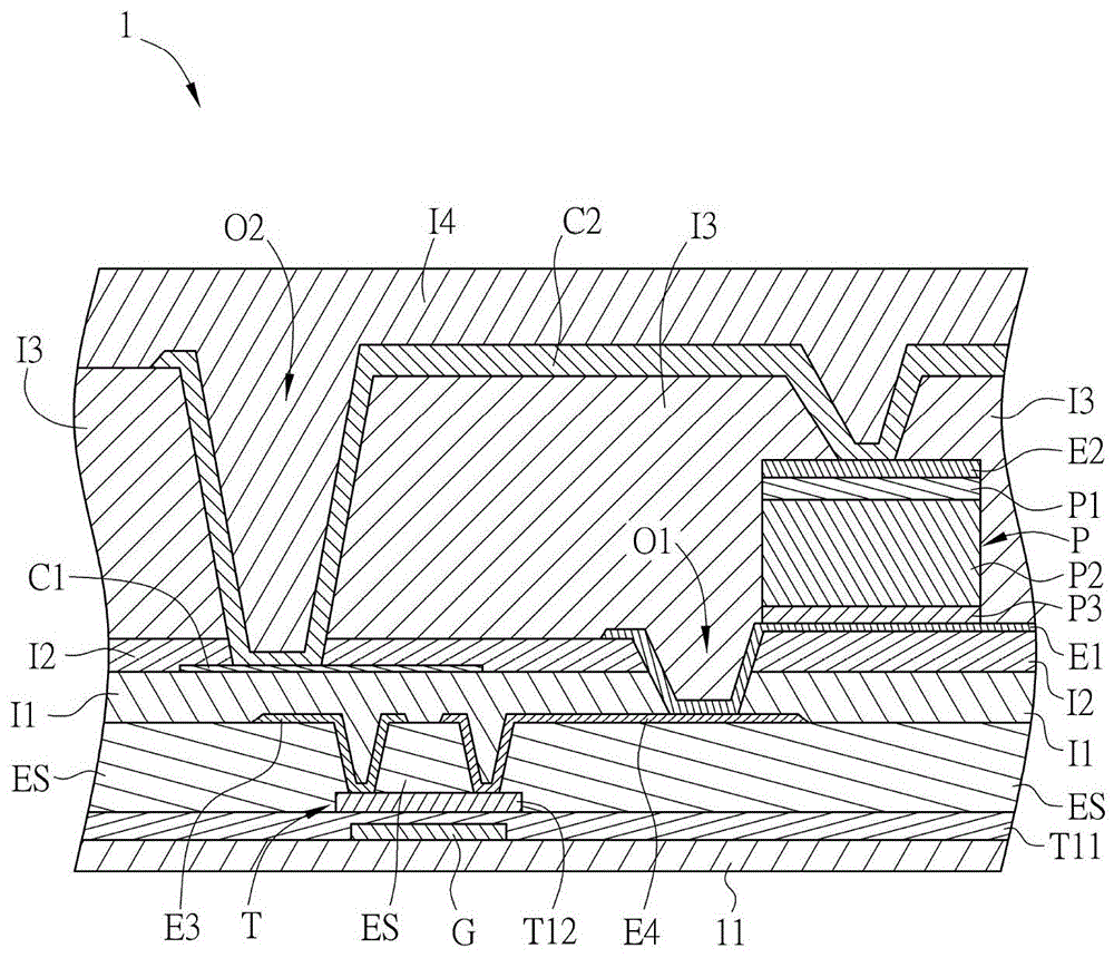
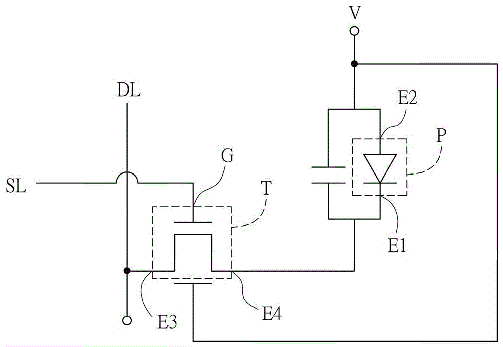
[0050] Please also refer to Figure 1A and Figure 1B As shown, among them, Figure 1A It is a schematic structural diagram of an image sensing pixel in an active matrix image sensing panel 1 according to a preferred embodiment of the present invention, and Figure 1B for Figure 1A The equivalent circuit diagram of the image sensor pixel.
[0051] The active matrix image sensing panel 1 includes a plurality of image sensing pixels disposed on a substrate 11 . In practice, the substrate 11 can be a light-transmitting material, such as glass, quartz or the like, plastic, rubber, glass fiber or other polymer materials, preferably a borate alkali-free glass substrate ( aluminum silicate glass substrate). The substrate 11 can a...
PUM
 Abstract
Description
Claims
Application Information
 - R&D Engineer
- R&D Manager
- IP Professional
- Industry Leading Data Capabilities
- Powerful AI technology
- Patent DNA Extraction
Browse by: Latest US Patents, China's latest patents, Technical Efficacy Thesaurus, Application Domain, Technology Topic, Popular Technical Reports.
© 2024 PatSnap. All rights reserved.Legal|Privacy policy|Modern Slavery Act Transparency Statement|Sitemap|About US| Contact US: help@patsnap.com


