Method for manufacturing integrated photolithography plate and method for sorting LED chip grains
A production method and technology for photolithography, which are applied in the photomechanical process of photomechanical processing of originals, optics, and pattern surfaces, etc., can solve the problems that various specifications of grains cannot be sorted quickly, efficiently and easily.
- Summary
- Abstract
- Description
- Claims
- Application Information
AI Technical Summary
Problems solved by technology
Method used
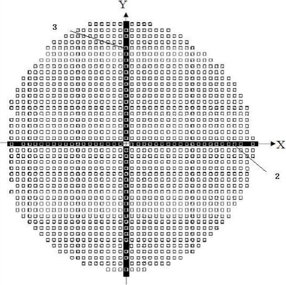
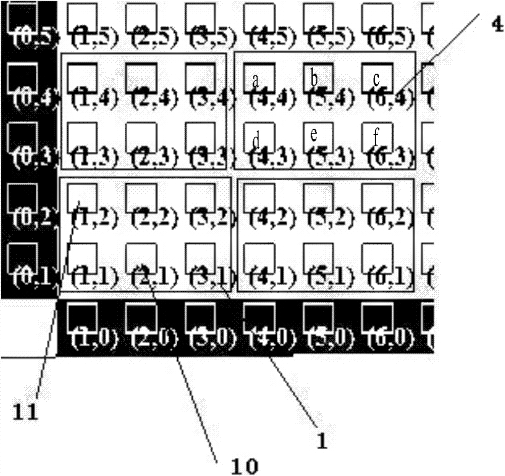
Image

Examples
Embodiment Construction
[0021] The embodiments of the present invention will be described in detail below with reference to the accompanying drawings, but the present invention can be implemented in many different ways defined and covered by the claims.
[0022] The invention provides a manufacturing method of an integrated photolithography board and a sorting method of LED chips. The method designs the distribution positions of crystal grain templates with different patterns and specifications on the integrated photolithography board on corresponding coordinate points of the template. After using the integrated photolithography board to make crystal grains, the positions of different graphics and different specifications of grains are fixed, and by modifying the Bin value of the grains at the corresponding positions, the sorting of LED chips can be completed through the sorting machine, while No need to rely on CCD cameras, which improves the efficiency and accuracy of sorting.
[0023] The inventio...
PUM
 Abstract
Description
Claims
Application Information
 - R&D
- Intellectual Property
- Life Sciences
- Materials
- Tech Scout
- Unparalleled Data Quality
- Higher Quality Content
- 60% Fewer Hallucinations
Browse by: Latest US Patents, China's latest patents, Technical Efficacy Thesaurus, Application Domain, Technology Topic, Popular Technical Reports.
© 2025 PatSnap. All rights reserved.Legal|Privacy policy|Modern Slavery Act Transparency Statement|Sitemap|About US| Contact US: help@patsnap.com