
Method for preparing molybdenum disulfide film for field emission device

A field emission device, molybdenum disulfide technology, applied in the manufacture of discharge tubes/lamps, electrical components, cold cathode manufacturing, etc., can solve the problem that the two-dimensional atomic crystal material MoS2 is rarely studied, and achieve rich spatial geometric edges , large specific surface area, and the effect of reducing the applied electric field

Inactive Publication Date: 2014-07-16
TSINGHUA UNIV
View PDF4 Cites 14 Cited by
  • Summary
  • Abstract
  • Description
  • Claims
  • Application Information

AI Technical Summary

Problems solved by technology

Two-dimensional atomic crystal material MoS suitable for high-performance field emission devices 2 little research

Method used


Image

  • Method for preparing molybdenum disulfide film for field emission device
  • Method for preparing molybdenum disulfide film for field emission device
  • Method for preparing molybdenum disulfide film for field emission device

Examples


Embodiment Construction

[0024] Embodiments of the present invention are described in detail below, examples of which are shown in the drawings, wherein the same or similar reference numerals designate the same or similar elements or elements having the same or similar functions throughout. The embodiments described below by referring to the figures are exemplary and are intended to explain the present invention and should not be construed as limiting the present invention.

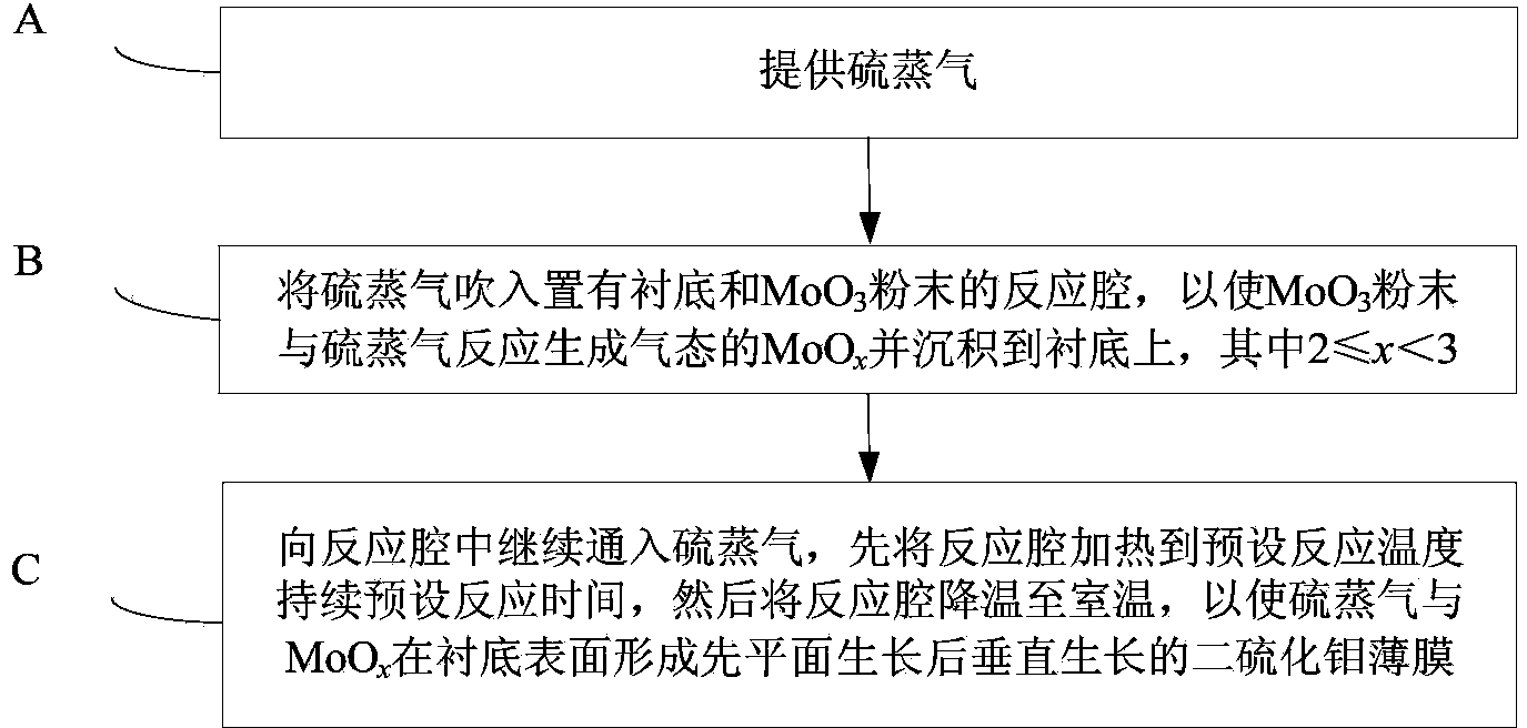
[0025] The present invention proposes a method for preparing a molybdenum disulfide thin film for field emission devices, such as figure 1 shown, including:

[0026] A. Provide sulfur vapor.

[0027] Specifically, the sulfur vapor can be obtained by sublimation of sulfur powder.

[0028] B. Blowing sulfur vapor into the substrate and MoO 3 Powder reaction chamber to make MoO 3 The powder reacts with sulfur vapor to form gaseous MoO x and deposited on the substrate, where 2≤x<3.

[0029] Specifically, sulfur vapor can be blo...


PUM


Abstract

The invention discloses a method for preparing a molybdenum disulfide film for a field emission device. The method comprises the following steps: providing sulfur vapor; blowing the sulfur vapor into a reaction cavity with a substrate and MoO3 powder, so that the MoO3 powder reacts with the sulfur vapor to generate gaseous MoOx and deposit on the substrate, wherein x is smaller than 3 and greater than or equal to 2; continuing to introduce the sulfur vapor into the reaction cavity; and firstly heating the reaction cavity to the preset reaction temperature to last for preset reaction time, and then cooling the reaction cavity to room temperature and lasting for second reaction time, so that the molybdenum disulfide film which firstly grows in a plane and then vertically grows is formed by the sulfur vapor and MoOx on the surface of the substrate. The preparation method of the molybdenum disulfide film disclosed by the invention is simple and feasible, and the obtained MoS2 film is good in field emission properties.

Description

technical field [0001] The invention relates to the technical field of chemical vapor deposition, in particular to a method for preparing a molybdenum disulfide thin film used for a field emission device. Background technique [0002] Field emission (FED) is to apply a high-intensity electric field on the surface of metal or semiconductor, and make electrons enter the vacuum through the tunnel effect. Compared with thermionic emission, field emission cold cathodes have the advantages of low power consumption and fast response. [0003] Early field emission cathode materials usually use M O , W and other high-melting point metals and Si and other semiconductor materials, and prepare them into pointed cones to reduce the required external electric field strength, but this cathode material emits a small current, unstable performance, complex preparation process, and high cost. to the application level. The field enhancement of the thin film edge structure is larger than that...

Claims


Application Information

Patent Timeline
IPC IPC(8): C23C16/44C23C16/30
CPCH01J1/304C23C16/305C23C16/4488C23C16/45523H01J9/025H01J2201/30449
Inventor 吴华强袁硕果李寒钱鹤
Owner TSINGHUA UNIV
Learn More