Crystalline silicon solar cell matrix back electrode

A technology of solar cells and back electrodes, applied in circuits, photovoltaic power generation, electrical components, etc., to achieve the effect of lower unit consumption and lower unit consumption

Inactive Publication Date: 2016-05-18
ENVIRONMENTAL NATURAL CHEM JIANGSU
View PDF5 Cites 0 Cited by
  • Summary
  • Abstract
  • Description
  • Claims
  • Application Information

AI Technical Summary

Problems solved by technology

[0005] In order to solve the above-mentioned problems, the present invention provides a matrix type back electrode of a crystalline silicon solar cell, which reduces the consumption of back silver; has better contact with the back aluminum and increases the printing of the back field area, which better improves the current and voltage; at the same time, it also better controls the superposition of the back electrode and the back electric field

Method used


Image

  • Crystalline silicon solar cell matrix back electrode
  • Crystalline silicon solar cell matrix back electrode

Examples


Embodiment

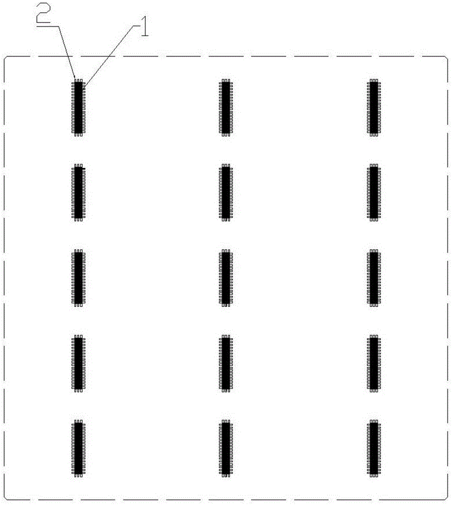
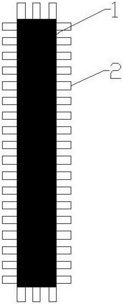
[0018] Embodiment: A matrix-type back electrode of a crystalline silicon solar cell, the crystalline silicon solar cell is a polycrystalline 156 solar cell, the back electrode 1 has fifteen segments, and the fifteen segment back electrodes are arranged in a matrix of five rows and three columns One row of back electrodes is located in the middle of the back of the cell, and the other two rows of back electrodes are each 52 mm away from the middle row of back electrodes (referring to the distance between the center lines of each row of back electrodes). A plurality of frame lines 2 are connected to the edges of the segment back electrodes, and the frame lines are evenly distributed around the back electrode at intervals, and the edges of the back electrodes and the frame lines are in contact with the back electric field.

[0019] The back electrodes in each segment are rectangular vertical strips with a length of 18 mm and a width of 2.3 mm, and the distance between the back ele...

experiment example

[0022] Experimental example: matrix back electrode of the present invention

[0023] Put the screen plate into the printing machine, install the scraper, ink return knife, and add slurry, adjust the printing parameters to ensure that the printed back electrode pattern is good, measure the wet weight, and the results are as follows:

[0024] sampling

1

2

3

4

5

average

wet weight (g)

0.033

0.035

0.037

0.036

0.034

0.035

[0025] The situation of measuring its electrical performance parameters under the conditions of AM1.5, light intensity 1000W, and 25°C is:

[0026] Voc (open circuit voltage)


PUM


Abstract

The invention discloses matrix back electrodes for a crystalline silicon solar cell. The crystalline silicon solar cell is a polycrystalline cell piece. 15 back electrodes are arranged in a five-line three-row matrix shape. One row of back electrodes are disposed in the middle of the cell piece back, and the other two rows of back electrodes are 52 millimeters away from the middles respectively. Each back electrode is in a vertical bar shape, and a plurality of frame lines are connected with the edges of all the back electrodes and cover the peripheries of the back electrodes uniformly at intervals. The edges of the back electrodes and the frame lines are in contact with a back electric field. By means of the matrix back electrodes, the back silver consumption is reduced, the contact with back aluminum is good, the back field printing area is increased, the current and the voltage are improved, and the stacking of the back electrodes and the back electric field is well controlled.

Description

technical field [0001] The invention belongs to the field of solar cell structures, and in particular relates to a back electrode structure of polycrystalline 156 cells. Background technique [0002] A solar cell is a device that directly converts light energy into electrical energy. Due to its cleanliness, pollution-free, inexhaustible and inexhaustible, it has attracted more and more attention. [0003] At present, silicon solar cells are widely used, and its manufacturing process has also been standardized. The main steps are: chemical cleaning and surface structuring (texturing)-diffusion junction-peripheral etching-deposition of anti-reflection film-screen printing-sintering . Among them, the screen printing first prints the back electrode, the paste is Ag paste, the back electric field is printed after drying, the paste is Al paste, and the front electrode is printed after being turned over by a flipper after drying, and the paste is Ag paste. For polycrystalline 156...

Claims


Application Information

Patent Timeline
Patent Type & Authority Patents(China)
IPC IPC(8): H01L31/0224
CPCH01L31/022433H01L31/022441H01L31/0682Y02E10/50
Inventor 白海赞胡中
Owner ENVIRONMENTAL NATURAL CHEM JIANGSU
Why Eureka
Try Eureka