A structure and monitoring method for monitoring engraving-back depth

A deep, wafer-based technology, applied in electrical components, circuits, semiconductor/solid-state device testing/measurement, etc., can solve problems such as large maintenance costs, increased initial testing costs, and high stepper prices, achieving cost reduction and better performance. Practicality and simple operation

Active Publication Date: 2016-12-21
CSMC TECH FAB2 CO LTD
View PDF8 Cites 0 Cited by
  • Summary
  • Abstract
  • Description
  • Claims
  • Application Information

AI Technical Summary

Problems solved by technology

For the second method, with the reduction of the critical size of the device, the requirements for the probe of the step meter are getting higher and higher, and the price of the step meter with high precision is extremely expensive, which undoubtedly increases the initial cost of testing. It also requires high maintenance costs

Method used


Image

  • A structure and monitoring method for monitoring engraving-back depth
  • A structure and monitoring method for monitoring engraving-back depth
  • A structure and monitoring method for monitoring engraving-back depth

Examples


Embodiment Construction

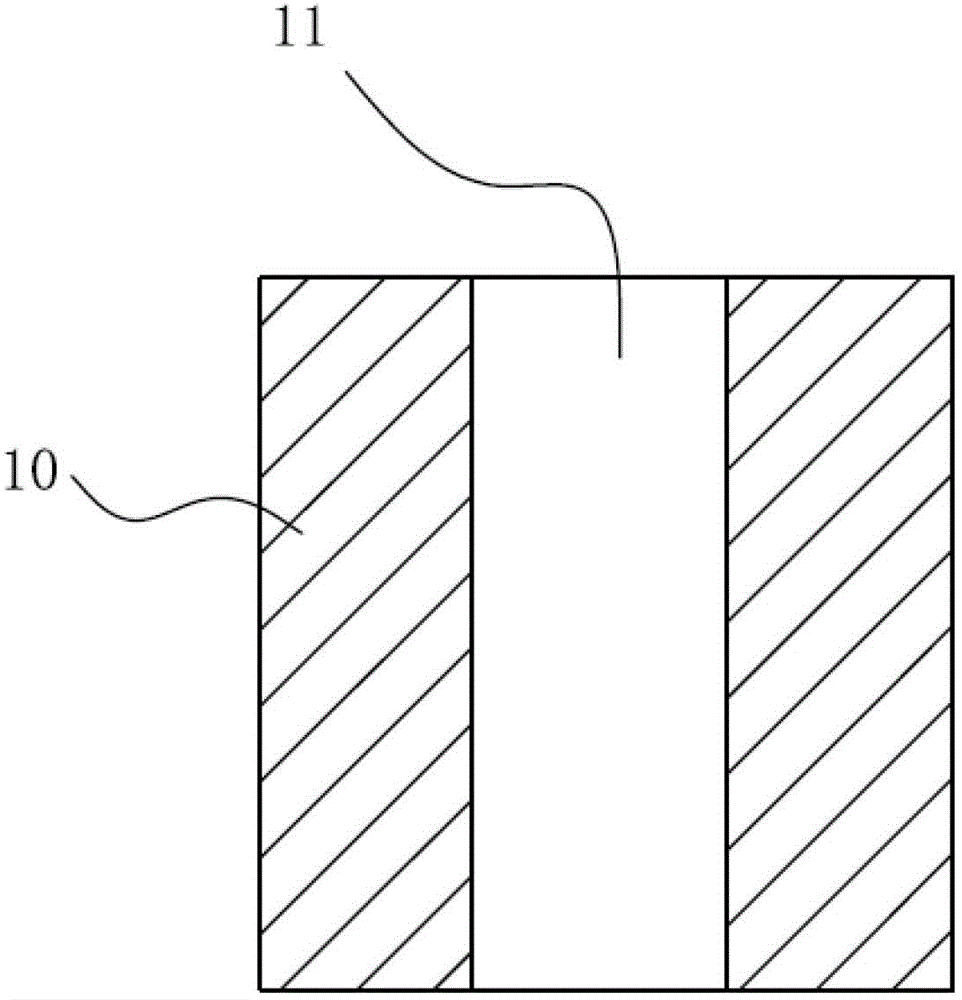
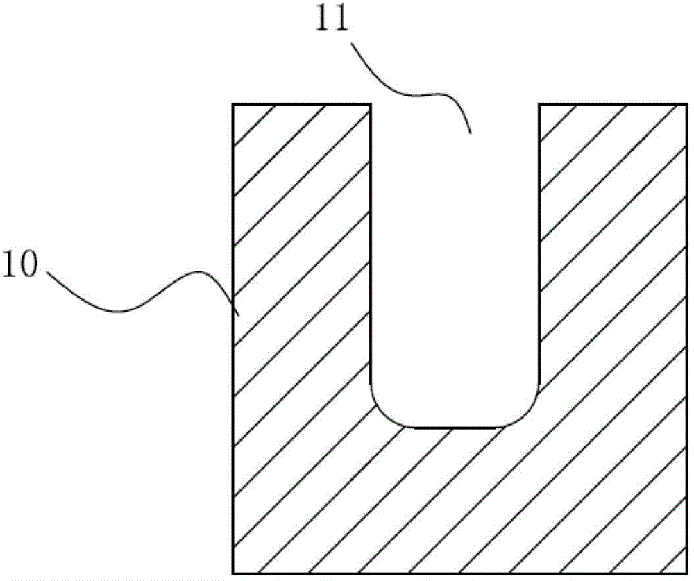
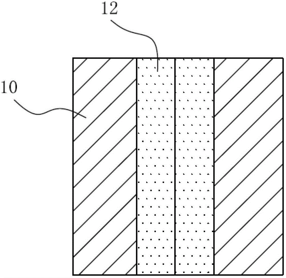
[0037] As mentioned in the background, the existing monitoring methods for polysilicon etch-back depth of trench DMOS devices are either to perform destructive testing on wafer chips, or to use expensive instruments for testing, both of which are costly , The monitoring method is too complicated and other defects, so it cannot meet the requirements of assembly line production.

[0038] Therefore, aiming at the defects in the prior art, the present invention proposes a monitoring structure and method for engraving back depth. The monitoring structure is made in the non-element area of ​​the wafer substrate, and is a groove with a special structure. After the groove undergoes a polysilicon etching process, the polysilicon can be divided into a blank area and a filling area in the groove. And at the junction of the two regions, an obvious polysilicon inflection point appears. Using the position where the inflection point appears in the monitoring structure, the corresponding etc...


PUM


Abstract

The invention relates to a structure for monitoring an etching back depth and a monitoring method. According to the monitoring structure, the structure is a groove that is manufactured at a wafer non-element zone and has a trapezoidal surface cross section. The monitoring method is characterized in that the trapezoidal groove is used to obtain a distribution inflection point of a sediment after the etching back process; and according to the inflection point position, whether the etching back depth meets the requirement or not can be determined. According to the monitoring method, only simple auxiliary equipment is needed. Therefore, compared with the original monitoring means, the monitoring method enables the cost to be substantially lowered; the operation is simple and the result is accurate; and the method is suitable for assembly line type on-line monitoring. In addition, the monitoring structure only occurs at the intermediate process of the whole DMOS device manufacturing technology and thus no negative effect is caused on the finished product. The structure has the high practicability.

Description

technical field [0001] The invention relates to the field of manufacturing semiconductor devices, in particular to a structure and a monitoring method for monitoring the etching-back depth in the etching-back process. Background technique [0002] A DMOS (Double Diffused MOS) transistor is a transistor of the MOSFET (Metal Oxide Semiconductor Field Effect Transistor) type that uses two sequential diffusion steps aligned on the same edge to form the channel region of the transistor. DMOS transistors are usually high-voltage, high-current devices used as discrete transistors or components in power integrated circuits. DMOS transistors can deliver high current per cell area with low forward voltage drop. [0003] A specific type of DMOS transistor is the so-called trench DMOS transistor, in which the channel appears on the inner wall of the trench extending from the source to the drain, and the gate is formed in the trench. Polysilicon-filled trenches aligned with a thin oxid...

Claims


Application Information

Patent Timeline
Patent Type & Authority Patents(China)
IPC IPC(8): H01L21/66
CPCH01L22/12H01L22/26H01L22/34
Inventor 卞铮
Owner CSMC TECH FAB2 CO LTD
Why Eureka
Try Eureka