Punch-through IGBT and manufacturing method thereof

A production method and a punch-through technology, which is applied in semiconductor/solid-state device manufacturing, semiconductor devices, electrical components, etc., can solve difficult problems and achieve the effects of reducing process difficulty, increasing thickness, and reducing the risk of splinters

Inactive Publication Date: 2014-06-11
INST OF MICROELECTRONICS CHINESE ACAD OF SCI +2
View PDF0 Cites 3 Cited by
  • Summary
  • Abstract
  • Description
  • Claims
  • Application Information

AI Technical Summary

Problems solved by technology

[0007] However, the methods for fabricating punch-through IGBTs in the prior art are quite difficult

Method used


Image

  • Punch-through IGBT and manufacturing method thereof
  • Punch-through IGBT and manufacturing method thereof
  • Punch-through IGBT and manufacturing method thereof

Examples


Embodiment Construction

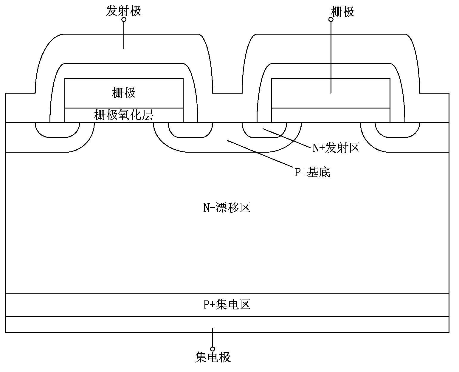
[0038] As mentioned in the background art section, in the prior art, there is a problem of high manufacturing difficulty when manufacturing punch-through IGBTs.

[0039] The inventors have found that there are two methods for fabricating the punch-through IGBT in the prior art: one is to fabricate the punch-through IGBT through an epitaxial process; the other is to fabricate the punch-through IGBT through a diffusion or ion implantation process.

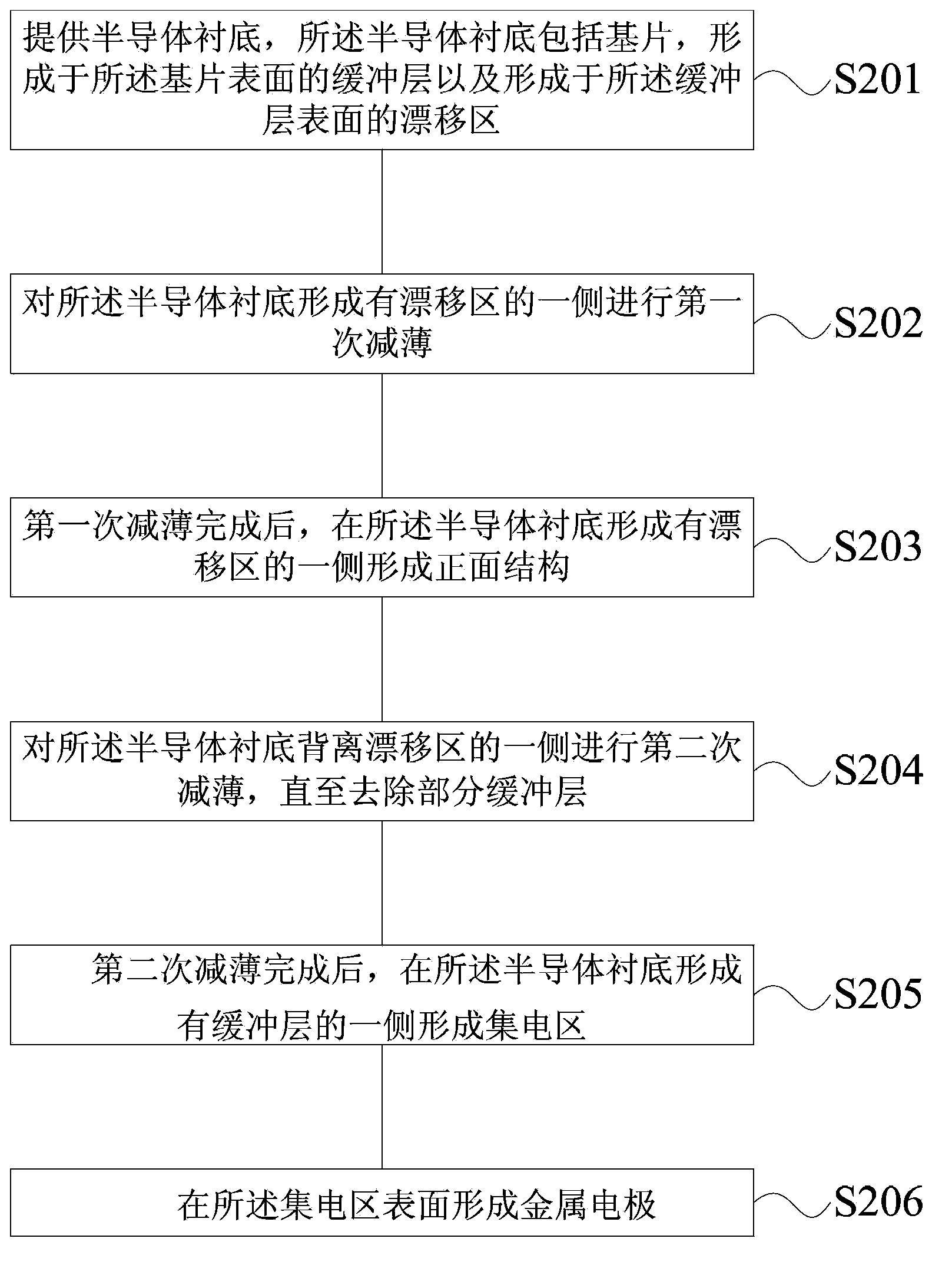
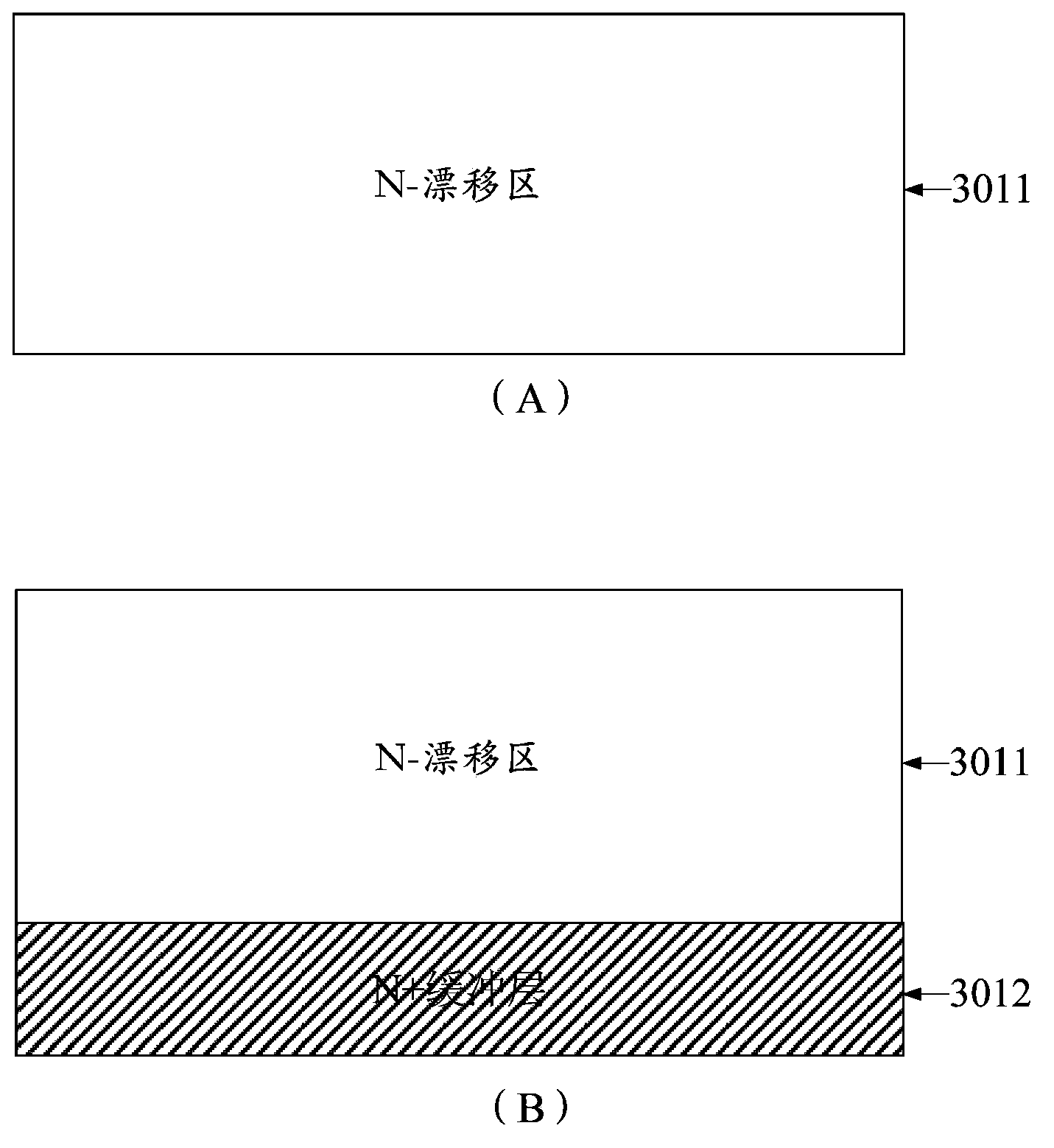
[0040] For the method of making punch-through IGBT by epitaxial process, it specifically includes: providing a P-type silicon substrate, epitaxially growing an N-type buffer layer on the surface of the P-type silicon substrate; and then epitaxially growing an N-type buffer layer on the surface of the N-type buffer layer Drift region; then make a front structure on the surface of the N-type drift region; finally thin the back of the P-type silicon substrate to form a collector region. The drift region and buffer layer in this method a...


PUM


Abstract

The invention discloses a punch-through IGBT and a manufacturing method of the punch-through IGBT. The method comprises the steps of providing a semiconductor substrate, wherein the semiconductor substrate comprises a substrate, a buffer layer formed on the surface of the substrate and a drift region formed on the surface of the buffer layer; conducting first-time thinning on the side, provided with the shift region, of the semiconductor substrate; after the first-time thinning is completed, forming a front face structure on the side, provided with the shift region, of the semiconductor substrate; conducting second-time thinning on the side, away from the shift region, of the semiconductor substrate until part of buffer layer is removed; after second-time thinning is completed, forming a collector region on the side, provided with the buffer layer, of the semiconductor substrate, and forming a metal electrode on the surface of the collector region. According to the manufacturing method of the punch-through IGBT, the manufacturing difficulty of the punch-through IGBT is reduced, and particularly the manufacturing difficulty of the thinner low-medium voltage punch-through IGBT is reduced.

Description

technical field [0001] The invention belongs to the field of semiconductor devices, in particular to a punch-through IGBT and a manufacturing method thereof. Background technique [0002] The modern high-voltage semiconductor device IGBT is a third-generation power electronic product with a voltage level covering 600V~6500V. Due to its high operating frequency, fast switching speed, and high control efficiency, it is widely used in household appliances, industrial frequency conversion, smart grids, and rail transit. and electric vehicles. [0003] IGBT is divided into non-punch-through type and punch-through type, such as figure 1 As shown, the non-punch-through IGBT includes: a drift region; [0004] A front structure, the front structure is formed on the front of the drift region, including an emitter region and a base region, and corresponding emitters and gates; [0005] The back structure, which is formed on the back of the drift region, includes a collector region a...

Claims


Application Information

Patent Timeline
Patent Type & Authority Applications(China)
IPC IPC(8): H01L21/331H01L29/739H01L29/06
CPCH01L29/66325H01L29/7393
Inventor 喻巧群朱阳军胡爱斌陆江
Owner INST OF MICROELECTRONICS CHINESE ACAD OF SCI
Why Eureka
Try Eureka