Electrochromic mirror
An electrochromic and electrode technology, applied in the direction of instruments, optical observation devices, layered products, etc., can solve the problems of increased density, obstruction, and inability to obtain anti-glare effects
- Summary
- Abstract
- Description
- Claims
- Application Information
AI Technical Summary
Problems solved by technology
Method used
Image
Examples
Embodiment
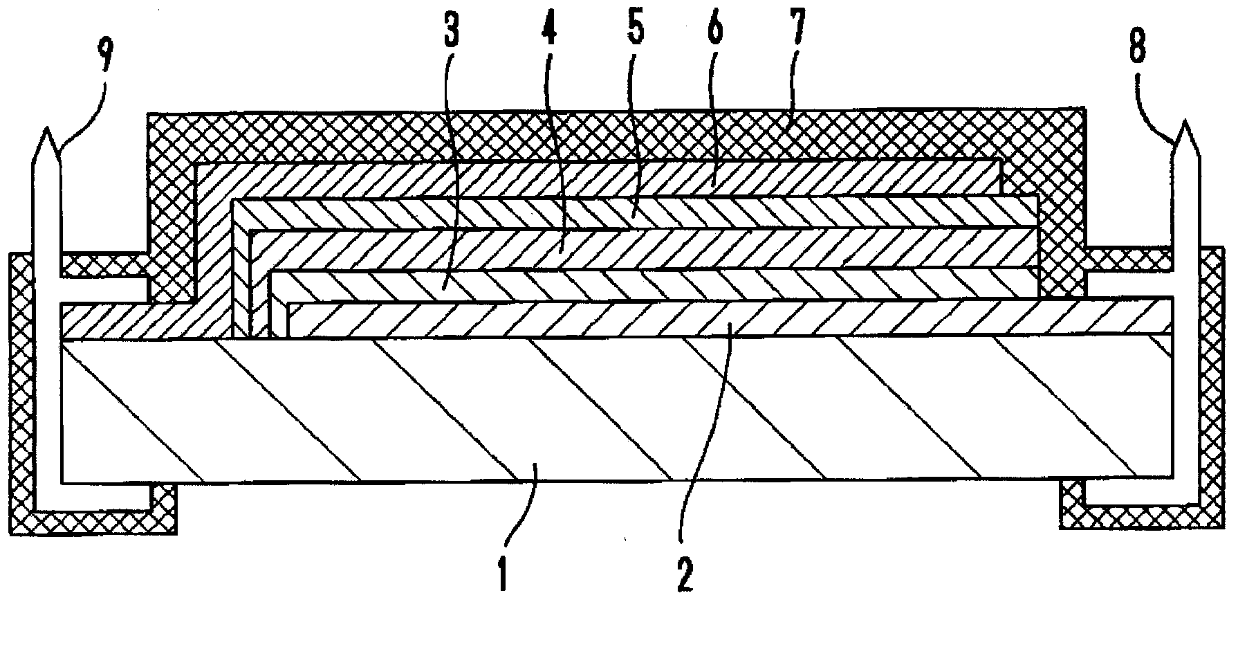
[0074] by ion plating with The film thickness is evaporating ITO on the glass substrate to form a transparent electrode film with a transmittance of 90% or more and a sheet resistance of 10Ω / □ or less. Then, by ion plating in the same way, the total film thickness is (IrO 2 : SnO 2 : ) by evaporation of IrO 2 +SnO 2 And form an oxidation chromogenic film with a transmittance of more than 80%. Then similarly by ion plating with The film thickness evaporated Ta 2 o 5 And form an electrolyte membrane with a transmittance of 90% or more. by electron beam evaporation to The film thickness evaporates WO on the above electrolyte membrane 3 And form a reduced chromogenic layer with a transmittance of 95% or more. On the above-mentioned reduced chromogenic layer, in contact with it, by a resistance heating evaporation method or the like to Al is vapor-deposited to a thickness of 10000 Ω to form a reflective and electrode film with a sheet resistivity of 10Ω / □ or hi...
PUM
| Property | Measurement | Unit |
|---|---|---|
| thickness | aaaaa | aaaaa |
| thickness | aaaaa | aaaaa |
| thickness | aaaaa | aaaaa |
Abstract
Description
Claims
Application Information
 - R&D
- Intellectual Property
- Life Sciences
- Materials
- Tech Scout
- Unparalleled Data Quality
- Higher Quality Content
- 60% Fewer Hallucinations
Browse by: Latest US Patents, China's latest patents, Technical Efficacy Thesaurus, Application Domain, Technology Topic, Popular Technical Reports.
© 2025 PatSnap. All rights reserved.Legal|Privacy policy|Modern Slavery Act Transparency Statement|Sitemap|About US| Contact US: help@patsnap.com


