
A 3D chip redundant TSV fault-tolerant structure with the function of transferring signals

A through-silicon via, 3D technology, applied in the direction of electrical components, reliability improvement and modification, electrical solid-state devices, etc., can solve problems such as signal failure to transmit normally, and achieve the effects of solving signal failure, cost reduction, and high fault tolerance

Inactive Publication Date: 2016-07-06
HEFEI UNIV OF TECH
View PDF2 Cites 0 Cited by
  • Summary
  • Abstract
  • Description
  • Claims
  • Application Information

AI Technical Summary

Problems solved by technology

[0008] In order to avoid the shortcomings in the above-mentioned prior art, the present invention provides a 3D chip redundant through-silicon hole fault-tolerant structure with the function of transferring signals, so as to solve the signal problem caused by the failure of the through-silicon hole in the three-dimensional integrated chip. The problem of not being able to transmit normally

Method used


Image

  • A 3D chip redundant TSV fault-tolerant structure with the function of transferring signals
  • A 3D chip redundant TSV fault-tolerant structure with the function of transferring signals
  • A 3D chip redundant TSV fault-tolerant structure with the function of transferring signals

Examples


Embodiment Construction

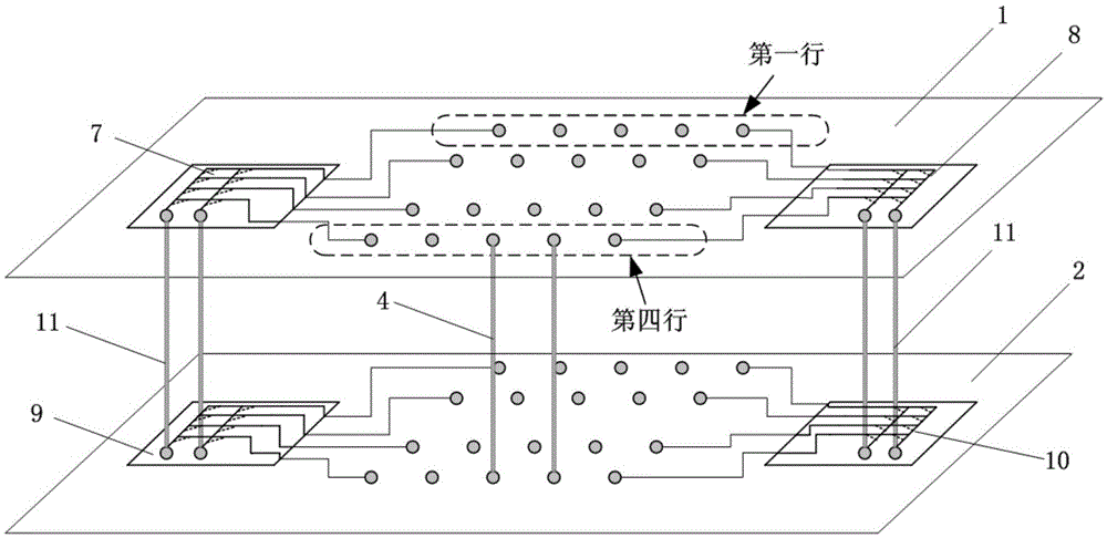
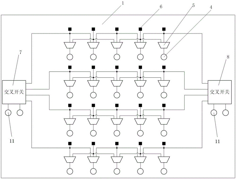
[0032] join Figure 1 to Figure 9, a 3D chip redundant TSV fault-tolerant structure with the function of transferring signals, the 3D chip includes an upper wafer 1 and a lower wafer 2; the upper wafer 1 and the lower wafer 2 are provided with vertical and horizontal Multiple rows and columns of circular holes 3; the circular holes 3 of the upper wafer 1 and the circular holes 3 of the lower wafer 2 are in one-to-one correspondence, and each pair of corresponding circular holes 3 of the upper wafer 1 and the lower wafer 2 passes through a The TSVs 4 are connected; on the upper wafer 1 and the lower wafer 2, the end of each TSV 4 is connected to a signal transmission terminal 6 through a multiplexer 5;

[0033] The upper wafer 1 is provided with two upper wafer cross switches, which are respectively a first upper wafer cross switch 7 and a second upper wafer cross switch 8; the lower wafer 2 is provided with two lower wafer cross switches, which are respectively The first lowe...


PUM


Abstract

The invention discloses a three-dimensional chip redundant TSV fault-tolerant structure with the function of transferring a signal. A three-dimensional chip comprises an upper-layer wafer and a lower-layer wafer. The upper-layer wafer and the lower-layer wafer are respectively provided with circular holes which are vertically and horizontally arrayed to form multiple rows and columns. Each circular hole in the upper-layer wafer and the corresponding circular hole in the lower-layer wafer are connected through a TSV. On the upper-layer wafer and the lower-layer wafer, the ends of all the TSVs are respectively connected with a signal transmission terminal through a multi-way selector. The upper-layer wafer and the lower-layer wafer are respectively provided with two crossbar switches, and all the crossbar switches are connected with the multi-way selectors. The crossbar switches of the upper-layer wafer are correspondingly connected with the crossbar switches of the lower-layer wafer through two redundant TSVs. The three-dimensional chip redundant TSV fault-tolerant structure has the advantages that the problem that a signal cannot be transmitted normally due to a TSV failure can be solved, the yield of the chip is effectively improved, hardware cost is low, the structure is simple, and the fault-tolerant capacity is high.

Description

technical field [0001] The invention relates to a 3D chip redundant through-silicon hole fault-tolerant structure with the function of transferring signals. Background technique [0002] With the development of integrated circuits, more and more devices are integrated on a single chip, and the circuits are developing in the direction of smaller and higher density. However, the problems of delay and power consumption caused by interconnect lines are becoming more and more prominent. Three-dimensional integrated circuit (3DIC) is an emerging technology. Due to its advantages in packaging density and flexibility of heterogeneous integration, it is considered to be an effective integrated circuit development technology. It usually uses vertical interconnection to replace ordinary Two-dimensional interconnection, vertical stacking reduces chip area and delay. [0003] Through-Silicon Vias (TSV) is an important technology in 3DIC. Through-Silicon Vias realizes signal transmission...

Claims


Application Information

Patent Timeline
Patent Type & Authority Patents(China)
IPC IPC(8): H03K19/003H01L23/538
Inventor 王伟张欢方芳陈田刘军吴玺
Owner HEFEI UNIV OF TECH
Learn More