Photochromic device
An electrochromic material and color-induced technology, applied in the direction of electric solid-state devices, photovoltaic power generation, electrical components, etc., can solve the problems of narrowing the color change range of electrochromic devices, achieve the expansion of color adjustable range, reduce production costs, The effect of simplifying the external circuit
- Summary
- Abstract
- Description
- Claims
- Application Information
AI Technical Summary
Problems solved by technology
Method used
Image
Examples
Embodiment 1
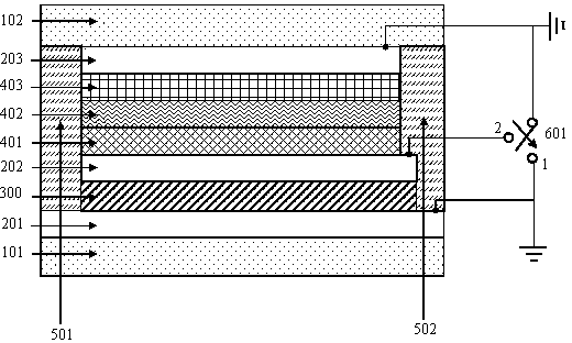
[0021] Implementation example 1: The specific implementation steps are as follows:
[0022] (1) if figure 2 As shown, a transparent conductive material layer 201, such as: ITO (In 2 o 3 :Sn), FTO (SnO:F) or AZO (ZnO:Al), its thickness is between 100nm-200nm, the sheet resistance is less than 30Ω / sq, and the light transmittance is greater than 85%;
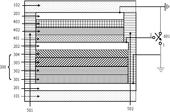
[0023] (2) Making an organic photoelectric conversion material layer 300 on the substrate 101 coated with a transparent conductive material 201 by vacuum evaporation method, including:
[0024] a) Cathode modification layer 301 (Cathode modification layer), such as: Bathocuproine (BCP), the thickness of which is between 5nm-50nm;
[0025] b) organic electron acceptor layer 302, such as: C 60 , its thickness is between 10nm-100nm;
[0026] c) The organic electron donor layer 303, such as: chloroaluminum phthalocyanine (ClAlPc), the thickness of which is between 10nm-100nm;
Embodiment 2
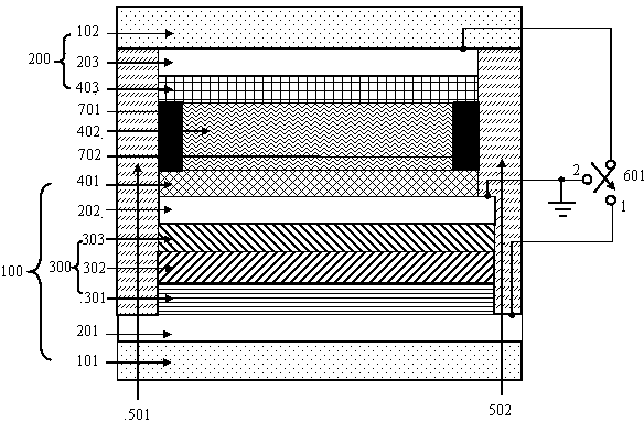
[0035] Implementation example 2: The specific implementation steps are as follows:
[0036] Such as image 3 As shown, (1) first make 100 parts of the device:
[0037] a) Utilize the magnetron sputtering method to make a transparent conductive material layer 201 on the transparent non-conductive substrate 101, such as: ITO (In 2 o 3 :Sn), FTO (SnO:F) or AZO (ZnO:Al), its thickness is between 100nm-200nm, the sheet resistance is less than 30Ω / sq, and the light transmittance is greater than 85%;
[0038] b) Make an organic photoelectric conversion material layer, including:
[0039] i. Anode modification layer 301: using spin-coating (spin-coating) to uniformly deposit poly(3,4-ethylenedioxythiophene):poly(styrene sulfonate) (ie PEDOT:PSS) on the transparent conductive material 201 layer, and at 120 o C for annealing treatment;
[0040] ii. Organic photoelectric conversion active layer 302: the polymer poly(2,60-4,8-bis(5-ethylhexylthienyl)benzo-[1,2-b;3,4-b]dithiophene-...
PUM
| Property | Measurement | Unit |
|---|---|---|
| thickness | aaaaa | aaaaa |
| transmittivity | aaaaa | aaaaa |
Abstract
Description
Claims
Application Information
 - R&D
- Intellectual Property
- Life Sciences
- Materials
- Tech Scout
- Unparalleled Data Quality
- Higher Quality Content
- 60% Fewer Hallucinations
Browse by: Latest US Patents, China's latest patents, Technical Efficacy Thesaurus, Application Domain, Technology Topic, Popular Technical Reports.
© 2025 PatSnap. All rights reserved.Legal|Privacy policy|Modern Slavery Act Transparency Statement|Sitemap|About US| Contact US: help@patsnap.com


